The proposed sinewave inverter UPS circuit is built using PIC16F72 microcontroller, some passive electronic components and associated power devices.
Data provided by: Mr. hisham bahaa-aldeen
Main Features:
The main technical features of the discussed PIC16F72 sinewave inverter may be evaluated from the following data:
Power output (625/800va) fully customization and can be upgraded to other desired levels.
Battery 12V/200AH
Inverter Output Volt : 230v (+2%)
Inverter Output Frequency : 50Hz
Inverter Output Waveform : PWM Modulated Sinewave
Harmonic Distortion : less than 3%
Crest Factor : less than 4:1
Inverter efficiency : 90% For 24v System, around 85% with 12v System
Audible Noise : less 60db At 1-meter
Inverter Protection Features
Low-battery Shut-down
Overload Shut-down
Output Short Circuit Shut-down
Low-battery Detection and Shutdown Feature
Beep Start initiated at 10.5v (beep At Every 3-sec)
Inverter Shut-down at around 10v (5 pulses of beep in every 2-sec)
Over Load : Beep Initiated at 120% Load (beep at the rate of 2-sec)
Inverter Shut-down at 130% Overload (5 pulses of beep in every 2-sec)
LED Indicators are provided for the following:
Inverter On
Low-battery - Flashing in Low battery mode with Alarm
Solid ON During Cut-OFF
Over Load - Flashing at Overload cut-off with Alarm
Solid ON During Cut-OFF
Charging mode - Flashing at Charging mode
Solid ON During Absorption
Mains Indication - LED On
Circuit Specifications
8-bit Microcontroller Based Control Circuit
H-bridge Inverter Topology
Mosfet Switching Fault Detection
Charging Algorithm : Mosfet PWM based switch mode Charger Controller 5-amp/15-amp
2-step Charging Step-1: Boost Mode (led Flash)
Step-2: Absorption Mode (led On)
DC Fan initialization for Internal Cooling During Charging/inv Operation
Circuit Diagram:
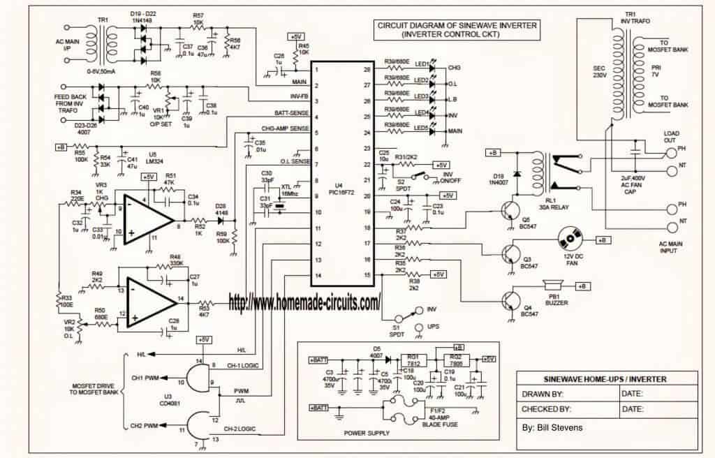
PIC Codes can be viewed HERE
PCB details are provided HERE
The following explanation provides the details of the various circuit stages involved in the design:
UPDATE:
You can also refer to this very easy to build pure sine wave Arduino based inverter circuit.
In Inverter Mode
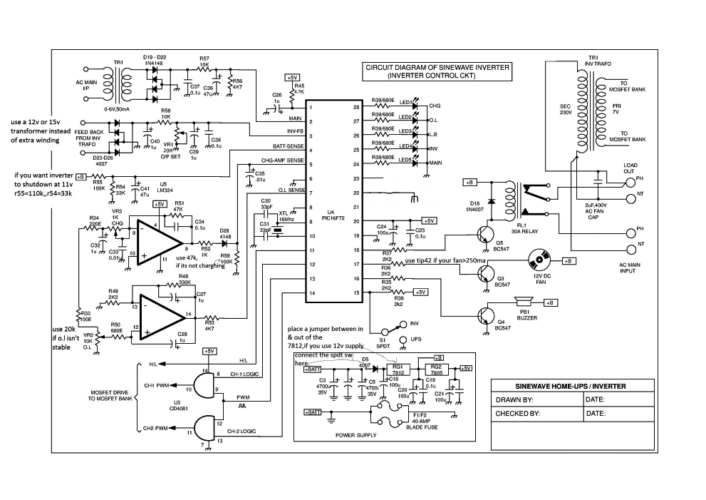
As soon as mains fails, the battery logic is detected at pin#22 of the IC which instantly prompts the controller section to switch the system in the inverter/battery mode.
In this mode the controller begins generating the required PWMs via its pin#13 (ccp out), however the PWM generation rate is implemented only after the controller confirms the logic level at pin#16 (INV/UPS switch).
If a high logic is detected at this pin (INV mode) the controller initiates a fully modulated duty cycle which is around 70%, and in case of a low logic at the indicated pinout of the IC, then the controller may be prompted to generate burst of PWMs ranging from 1% to 70% at a rate of 250mS period, which is termed as soft delay output while in the UPS mode.
The controller simultaneously with the PWMs also generates a "channel select" logic through pin#13 of the PIC which is further applied to pin#8 of the IC CD4081.
Throughout initial time period of the pulse (i.e 10ms) the pin12 of the PWM controller is rendered high such that the PWM can be obtained from pin10 of CD4081 exclusively and after 10mS, pin14 of controller is logic high and the PWM is accessible from pin11 of CD4081, as a result using this method a pair of anti-phased PWM becomes accessible to switch on the MOSFETs.
Aside from that a high logic (5V) becomes accessible from pin11 of the PWM controller, this pin turns high each time inverter is ON and ends up being low whenever inverter is OFF. This high logic is applied to pin10 of each the MOSFET drivers U1 and U2, (HI pin) to activate the high side MOSFETs of the two the mosfet banks.
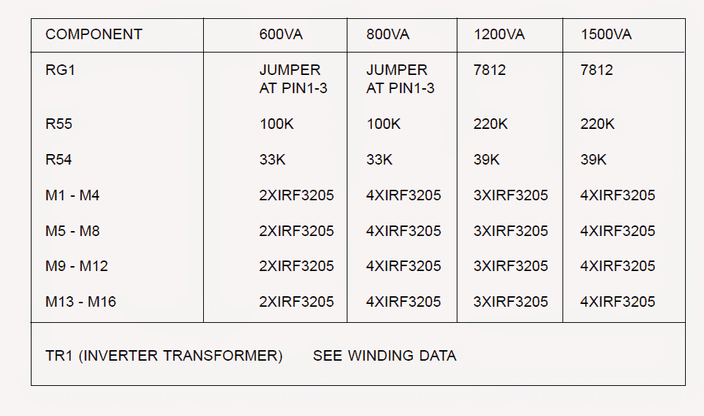
For upgrading the proposed microcontrollor Sinewave UPS, the following data may be used and implemented appropriately.
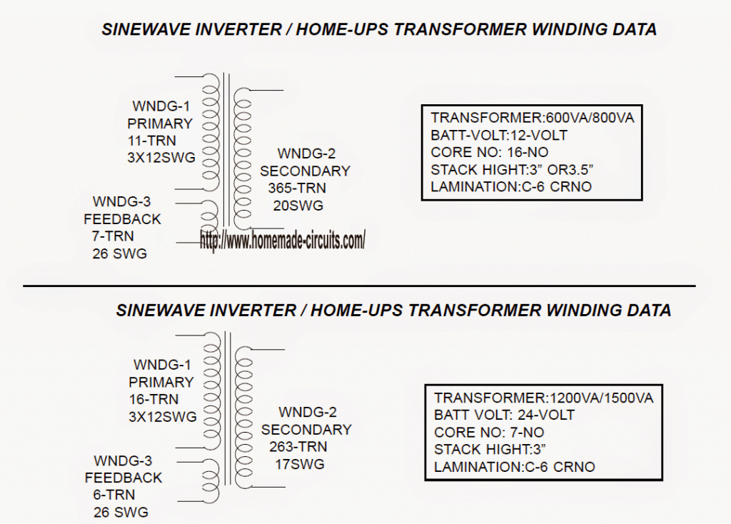
The following data supplies the full transformer winding details:
Feedback from Mr. Hisham:
Hi mr swagatam ,how are you?
I want to tell you that pure sine wave inverter schematic have some mistakes, 220uf bootstrap capacitor should be replaced with a (22uf or 47uf or 68uf),,,a 22uf capacitors which is connected between pin 1 and pin2 of the 2's ir2110 is wrong and should be removed, also a hex code called eletech. Hex should not be use cause its make inverter shutdown after 15 seconds with low battery led and buzer beeps, if you have big dc fan so the transistors should be replaced with a higher current,for mosfets safety a 7812 regulator is recommended to be connected to ir2110...also there's d14,d15 and d16 should not be connected to ground.
I have tested this inverter and its really pure sine wave,i have run a washing machine and its running silently without any noise, i have connected a 220nf capcitor in the ouput instead of 2.5uf, refrigerator is working too, i will share some pictures soon.
Best regards
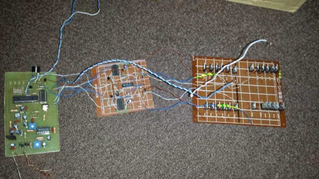
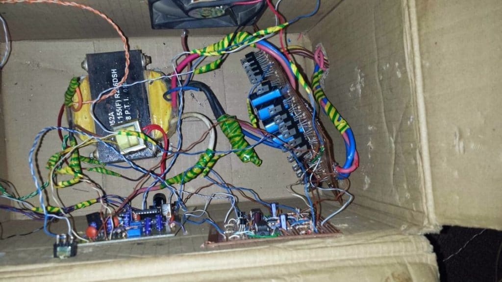
The schematic discussed in the above article was tested and modified with a few appropriate corrections by Mr. Hisham, as shown in the following images, viewers can refer to these for improving the performance of the same:
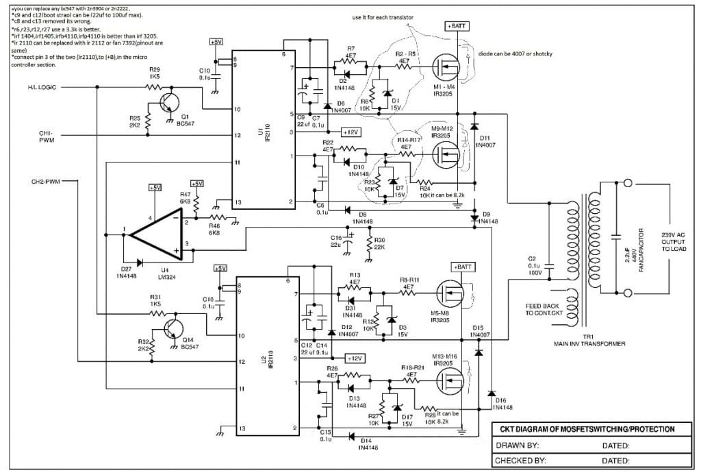
Now let us study how the mosfet switching stage can be built through the following explanation.
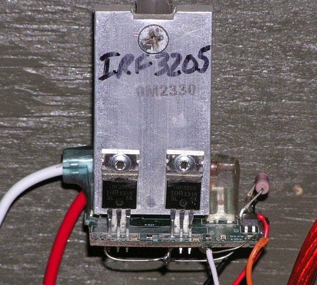
MOSFET Switching:
Check with MOSFET switching circuit diagram below:
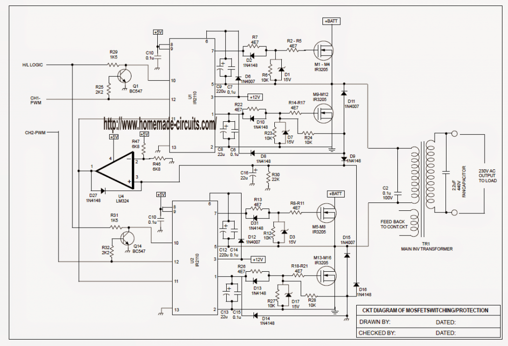
In this case U1 (IR2110) and U2 (IR2110) high side / low side mosfet driver are employed, check with data sheet of this IC to understand more. In this the two MOSFET banks with high side and low side MOSFETs are intended for transformer’s primary side switching.
In this case we are discussing the functioning of bank (applying IC U1) only since the supplementary bank driving does not differ from from each other.
As soon as the inverter is ON the controller renders the pin10 of U1 is logic high which subsequently activates the high side MOSFETs (M1 - M4) ON, PWM for channel-1 from pin10 of CD4081 is applied to pin12 of the drver IC (U1) and likewise it is administered to the base of Q1 via R25.
While the PWM is logic high the pin12 of U1 is also logic high and triggers the low side MOSFETs of bank 1(M9 - M12), alternately it launches the transistor
Q1 which correspondingly renders the pin10 voltage of U1 logic low, thereupon turning OFF the high side MOSFETs (M1 - M4).
Therefore it implies that by default the high logic from pin11 of the microcontroller gets switched ON for the high side MOSFETs among the two the mosfet arrays, and while the associated PWM is high the low side MOSFETs are turned ON and the high side MOSFETs are switched OFF, and through this way the switching sequence keeps repeating.
Mosfet Switching Protection
Pin11 of U1 can be used for executing the hardware locking mechanism of each of the drivers units.
By standard fixed mode this pin may be seen fixed with a low logic, but whenever under any circumstance the low side MOFET switching fails to initiate (let's assume through o/p short circuit or erroneous pulse generation at the output), the VDS voltage of low side MOSFETs can be expected to shoot up which immediately causes the output pin1 of comparator (U4) to go high and become latched with the help of D27, and render pin11 of U1 and U2 at high logic, and thereby toggle OFF the two the MOSFET driver stages effectively, preventing the MOSFETs from getting burnt and damaged.
Pin6 and pin9 is of +VCC of the IC (+5V), pin3 is of +12V for MOSFET gate drive supply, pin7 is the high side MOSFET gate drive, pin5 is the high side MOSFET receiving route, pin1 is the low side MOSFET drive, and pin2 is the low side MOSFET receiving path. pin13 is the ground of the IC (U1).
LOW BATTERY PROTECTION:
While the controller operates in the inverter-mode it repeatedly monitors the voltage at its pin4 (BATT SENSE), pin7 (OVER LOAD sense) and pin2 (AC MAIN sense).
Should the voltage at pin4 rise above 2.6V the controller would take no notice of it and may be seen escaping to supplementary sensing-mode, but as soon as the voltage here drops to around 2.5V the controller stage would prohibit its functioning at this point, switching OFF the inverter-mode such that the low battery LED turns ON and prompting the buzzer to beep.
OVER LOAD:
Over load protection is a mandatory functionality implemented in most inverter systems. Up here, in order to cut-of the inverter in the event the load goes beyond the safe load specifications, the battery current is first detected across the negative line (i.e the voltage drop across the fuse and negative path of the low side MOSFET bank) and this greatly reduced voltage (in mV) is proportionately intensified by the comparator U5 (composing of pins12,13 1nd 14) (make reference to circuit diagram).
This amplified voltage output from pin14 of comparator (U5) is rigged as inverting amplifier and applied to pin7 of the microcontroller.
The software compares the voltage with the reference, which is for this particular pin is 2V. Quite as talked over previously the controller senses the voltages in this pin besides operating the system in the inverter-mode, every time the load current augments the voltage at this pin builds up.
Whenever the voltage on pin7 of the controller IC is above 2V the process shuts off the inverter and switches to overload mode, shutting off the inverter, turning ON the overload LED and causing the buzzer to beep, which after 9-beeps prompts the inverter to switched-ON again, inspecting the voltage at pin7 for a second time, suppose in case the controller identifies pin7 voltage to be below 2V, it then operates the inverter on normal mode, other wise it disconnects the inverter yet again, and this process is known as the auto-reset-mode.
Like in this article we articulated beforehand that when in inverter-mode, the controller reads the voltage at its pin4 (for Low-batt), pin7 (for overload) and pin2 for AC main voltage status. We comprehend that the system may be functioning in twin mode (a) UPS mode,(b) inverter mode.
So before inspecting the pin2 voltage of PIC the routine before anything else confirms at what mode the unit may be working by sensing the high/lo logic at pin16 of the PIC.
Inverter to mains changeover (INV-MODE):
In this particular mode as soon as the AC main voltage is detected to be in the vicinity of 140V AC, the changeover action can be seen implemented, this voltage threshold is pre-settable by the user, implies that in cases where the pin2 voltage is above 0.9V, the controller IC may shut off the inverter and switch to mains-on mode, where the system examines the pin2 voltage to test the AC mains failure and maintain the charging process, which in this article we will be explaining later on.
Inverter to Battery changeover (UPS-MODE):
Within this setting each time the AC main voltage is in the vicinity of 190V AC the changeover may be seen enforcing to battery mode, this voltage threshold is also software pre-setteble, meaning when ever the pin2 volage is above 1.22V the controller may be expected to switch ON the inverter and switched to battery routine wherein the system inspects the pin2 voltage to verifies the AC mains absence and operates the charging schedule which we would be discussing further down in the article.
BATTERY CHARGING:
In the course of MAINs ON Battery charging may be seen initiated. As we may understand while in battery charging mode the system may be functioning using the SMPS technique, let us now understand the working principle behind it.
To charge the battery the output circuit (MOSFET and Inverter transformer) becomes effective in the form of a boost converter.
In this case all the low side MOSFETs of the two the mosfet arrays work in sync as a switching stage while the primary of the inverter transformer behave as an inductor.
As soon as all of the low side MOSFETs are switched-ON the electric power gets accumulated in the primary section of transformer, and as soon as the MOSFETs are OFF this accumulated electric power is rectified by the in-build diode inside the MOSFETs and the DC is kicked back to battery pack, the measure of this boosted voltage would depend on the ON-time of the low side MOSFETs or simply mark/space ratio of the duty cycle used for the charging process.
PWM WORKING
While the equipment may be conducting in the mains-on mode, the charging PWM (from pin13 of micro) is progressively augmented from 1% to highest specification, in case the PWM raises the DC voltage to the battery, the battery voltage too increases which results in a surge in the battery charging current.
The battery charging current is monitored across the DC fuse and negative rail of the PCB and the voltage is additionally intensified by the amplifier U5 (pin8, ppin9 and pin10 of the comparator) this amplified voltage or detected current are applied to the pin5 of microcontroller.
This pin voltage is scheduled in software in the form of 1V, as soon as the voltage in this pin is rises above 1V the controller may be seen restricting the PWM duty cycle until finally it's pulled down to below 1V, assuming the voltage on this pin is decreased to below 1V the controller would instantly begin improving the full PWM output, and the process may be expected to go on in this manner with the controller upholding the voltage on this pin at 1V and consequently the charging current limit.
SINEWAVE UPS TESTING AND FAULT FINDING
Construct the card thereby confirming each and every wiring, this includes LED connectivity, ON/OFF switch, feedback via inverter transformer, 6-volt mains sense to CN5, -VE of battery to card, +VE of battery to large heatsink.
Initially do not plug the transformer primary to the pair of small heat sinks.
Plug in battery +ve wire to PCB via MCB and 50-amp ammeter.
Prior to proceeding for the recommended testings be sure to check the +VCC voltage at the pins of
U1 - U5 in the following sequence.
U1:pin#8 and 9: +5V, pin#3: +12V, pin#6: +12V,
U2:pin#8 and 9: +5V, pin#3: +12V, pin6: +12V,
U3: pin14: +5V, U4: pin20: +5V, pin1:+5V, U5: pin4:+5V.
1) Power Up the battery MCB and check the ammeter and also be certain it doesn't jump beyond 1-amp. If the ampere shoots then remove U1 and U2 briefly and switch ON the MCB again.
2) Power ON by toggling the given ON/OFF switch of the inverter and check whether or not the relay clicks ON, illuminating the "INV" LED. If it doesn't then check the voltage at pin#18 of the PIC which is supposed to be 5V. If this is absent check components R37 and Q5, one of this may be faulty or incorrectly connected. If you find the "INV" LED not switching ON, check if the voltage at pin#25 of the PIC is 5V or not.
If the above situation is seen to be normally executing, go to the next step as described below.
3) Using an oscilloscope test pin#13 of the PIC by alternately switching ON/OFF the inverter switch, you can expect to see a well modulated PWM signal appearing at this pinout each time the inverter mains input is switched OFF, if not then you can assume the PIC to be faulty, coding not implemented correctly or the IC is badly soldered or inserted in its socket.
If you succeed in getting the expected modified PWM feed over this pin, go to pin#12/in#14 of the IC and check the availability of 50Hz frequency on these pins, if not would indicate some fault in the PIC configuration, remove and replace it. If you are to get affirmative response on these pins, go to the next step as I have explained below.
4) The next step would be to test pin#10/pin#12 of the IC U3 (CD4081) for the modulated PWMs which are finally integrated with the mosfet driver stages U1 and U2. Additionally you would be also required to check the potential differences at pin#9/pin#12 which is supposed to be at 3.4V approximately, and at pin#8/pin#13 may be verified to be at 2.5V. Similarly verify pin#10/11 to be at 1.68V.
In case you fail to identify the modulated PWM across the CD4081 output pins, then you would want to verify the tracks terminating to the relevant pins of the IC CD4081 from the PIC, which could be broken or somehow the obstructing the PWMs from the reaching U3.
If all is fine, let's move to the next level.
5) Next, attach the CRO with U1 gate, toggle the inverter ON/OFF and as done above verify the PWMs on this spot which are M1 and M4, and also the gates M9, M12, however don't be surprised if the PWM switching are seen out of phase M9/M12 as compared to M1/M4, that's normal.
If the PWMs are entirely absent on these gates, then you can check pin#11 of U1 which is expected to be low, and if found high would indicate that U1 may be running in the shut-down mode.
To confirm this situation check voltage at pin#2 of U5 which could be at 2.5V, and identically pin#3 of U5 could be at 0V or under 1V, if it's detected to be below 1V, then proceed and check R47/R48, but if the voltage is found to be above 2.5V then check D11, D9, along with mosfets M9, M12 and the relevant components around it to troubleshoot the persisting issue, until corrected satisfactorily..
In case where the pin#11 of U1 is detected low and still you are unable to find the PWMs from pin#1, and pin#7 of U1, then it's time to replace IC U1, which would possibly rectify the issue, which will prompt us to move to the next level below.
6) Now repeat the procedures exactly as done above for the gates of the mosfet array M5/M18 and M13/M16, the troubleshooting would be exactly as explained but with reference to U2 and the other complementary stages which may be associated with these mosfets
7) After the above testing and confirmation are completed, now it's finally time to hook up the transformer primary with the mosfet heatsinks as indicated in the sinewave UPS circuit diagram. Once this is configured, switch ON the inverter switch, adjust preset VR1 to hopefully access the required 220V regulated, constant sinewave AC across the output terminal of the inverter.
If you find the output to be exceeding this value or below this value, and void of the expected regulation, you may look for the following issues:
If the output is much higher, check voltage at pin#3 of the PIC which is supposed to be at 2.5V, if not then verify the feedback signal derived from the inverter transformer to connector CN4, further check voltage across C40, and confirm the correctness of the components R58, VR1 etc. until the issue is rectified.
8) After this attach an appropriate load to the inverter, and check the regulation, a 2 to 3 percent falter can eb considered normal, if still you fail a regulation, then check diodes D23----D26, you can expect one of these to be faulty or you may also try replacing C39, C40 for correcting the issue.
9) Once the above procedures are successfully completed, you can carry on by checking the LOW-BATT functioning. To visualize this try short circuiting R54 with the help of a pair of tweezers from the component side, which should instantly prompt the LOW-Batt LED to illuminate and the buzzer to beep for a period of around 9 seconds at the rate of a beep per second approximately.
In case the above does not happen, you may check pin#4 of the PIC, which should be normally at above 2.5V, and anything lower than this triggers the low batt warning indication. If an irrelevant voltage level is detected here check whether or not R55 and R54 are in a correct working order.
10) Next up it would be the overload tripping feature which would need to be confirmed. For testing you can select a 400 Wait incandescent bulb as the load and connect it with the inverter output. Adjusting VR2 the overload tripping should initiate at some point on the preset rotation.
To be precise, check the voltage at pin#7 of the PIC where under correct load conditions the voltage will be over 2V, and anything above this level will trigger overload cut-off action.
With a sample 400 watt, try varying the preset and try forcing an overload cut -off to initiate, if this does not happen, verify voltage at pin#14 of U5 (LM324) which is supposed to be higher than 2.2V, if not then check R48, R49, R50 and also R33 any of these could be malfunctioning, if everything's correct here simply replace U5 with a new IC and check the response.
Alternatively you can also try increasing the R48 value to around 470K or 560k or 680K etc and check if it helps solving the issue.
11) When the assessment of inverter processing is finished, experiment with the mains changeover.Keep the mode switch in inverter mode (keep CN1 open) switch-ON the inverter, hook up the mains wire to the variac, step up the variac voltage to 140V AC and check the inv to mains changeover triggering occurs or not. If you find no changeover in that case confirm the voltage at pin2 of microcontroller, it needs to be > 1.24V, in case the voltage is smaller than 1.24V then inspect the sensing transformer voltage (6V AC at its secondary) or take a look at the components R57,R56.
Now that the changeover shows up scale down the variac voltage to below 90V and examine the mains-to-inverter changeover action is established or not. The changeover ought to happen since now the voltage at pin2 of microcontroller is less than 1V.
12) Soon after the above assessment is completed, experiment with the mains-changeover in the UPS mode. Enabling the mode-switch in the UPS mode (keep CN1 shorted) start the inverter, link up the mains wire to the variac, increment the variac voltage to around 190V AC and observe the UPS-to-mains changeover strikes or not. Should there be no changeover action then simply take a look at the voltage at pin2 of microcontroller, it needs to be over 1.66V, as long as the voltage is lower than 1.66V then simply confirm the sensing transformer voltage (6V AC at its secondary) or perhaps inspect the elements R57,R56.
Right after the changeover pops up, scale back the variac voltage to 180V and find out whether the mains-to-UPS changeover comes about or not. The changeover ought to strike since now the voltage at pin2 of microcontroller could be witnessed to be over 1.5V.
13) Eventually take a look at the customized charging of the attached battery. Hold the mode switch in the inverter-mode, administer mains and step up the variac voltage to 230V AC, and determine the charging current which should rise smoothly in ammeter.
Fiddle with the charging current by varying VR3, so that the current variation could be witnessed varying in the middle of around 5-amp to 12/15-amp.
Just in case the charging current is seen to be much higher and not in a position to be scaled down at preferred level then you may try increasing the value of R51 to 100k and/or if still that does not improve the charging current to expected level then perhaps you can try decreasing the value of R51 to 22K, please bear in mind that once the sensed equivalent voltage at pin5 of microcontroller becomes at 2.5V the microcontroller may be expected to regulate the PWM and consequently the charging current.
In the course of the charging mode remember that, precisely the lower branch of MOSFETs (M6 -M12 / M13 - M16) are switching @8kHZ while the upper branch of MOSFETs are OFF.
14) Additionally you can inspect the operation of the FAN, FAN is ON each time the inverter is ON, and FAN could be seen switched OFF whenever the inverter is OFF. In a similar manner FAN is ON as soon as Charging is ON and FAN will be OFF when charging is OFF
