

In this post I have explained 6 simple, cheap class A power amplifier circuits which can be used for any small scale audio amplifier application.
By: Dhrubajyoti Biswas
1) Zero Negative Feedback Amplifier
This following data will detail how to build an amplifier having zero negative feedback which implies building a zero component amplifier. The amplifier will be single-ended and Class A.
To begin with, let us first lay down the circuit design of the proposed amplifier, as given under:

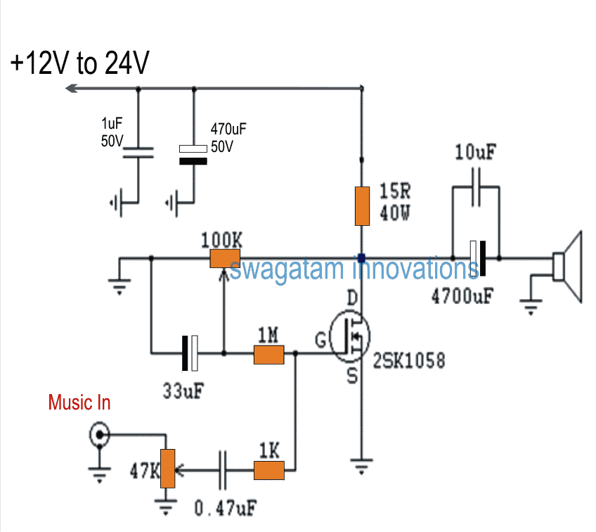
How to Build the Circuit
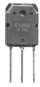
To build the circuit we need: A MOSFET, some capacitors and resistors and a sturdy power supply which has to be properly filtered using large filter capacitors. The amplifier we are building is built by incorporating the device 2SK1058 N-Channel MOSFET from Hitachi. The pin diagram is shown below:
The capacitors that we used in this experiment is that of Sprague. This is used to couple the input and on the output a large electrolytic along with polyester bypass capacitor of 10µF. To manage the load, we used four non-inductive wire wound resistors of 10W.
However, to achieve total resistance of 15 ohms, the resistors are wired on a series of two, which makes 30 ohms and furthermore setting up the sets in parallel. Please note, the device would be hot and susceptible to burning during idle mode, hence caution is utmost important.
Class-A can never be an ideal option for a high efficiency amplifier design, but as we are applying the idea in this setup, we had to use more than 20 Watts power to generate a modest 4.8 Watts audio. The heat-sink used for the mosfet was of 0.784 °C/W.
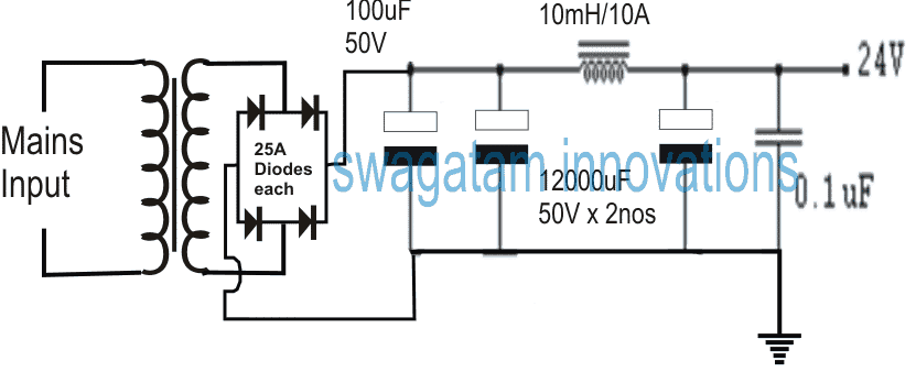
Power Supply
The power supply used for this single MOSFET class A power amplifier circuit is 18VAC and 160VA EI transformer attached to a bridge rectifier of 25 amp to generate DC power of 24 Volts.
To filter and smooth the power we used 10000µF capacitors and Hammond make 10mH choke of 5 amp over pi filter setting [Cap - Choke - Cap]. The bias was via a pot of 100K along with resistor of 1M.
Care should be taken to adjust the pot only for so long as half of the DC gets over the load resistors and MOSFET.

2) Easiest Class A Amplifier
The IRF511 (Q1) is wired like a most simple class-A audio-amplifier circuit, as shown in the figure below. Having zero gate bias employed, Q1 acts similar to a switch which is in the switched off state. In this condition no current moves from the load resistor, R2. Essentially, the voltage across Q1 and the load resistor have to be the same for the working of class-A amplifiers.

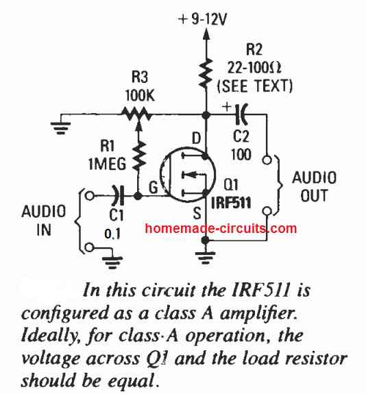
A 100K potentiometer (R3) along with a 1M fixed (R1) constitute a straightforward adjustable gate-bias circuit. If we put a a voltmeter across the Q1 drain and the ground of the circuit, and we fine-tune R3 to get a meter reading of half the power supply voltage.
Practically any resistor could be utilized in place of R2 provided that the maximum current and power ratings of the FET aren't surpassed. A resistor value of between 22 and 100 ohms can be a decent selection for testing. If high current supply is used, make sure to use an appropriate heat sink for the FET.
3) Class A Amplifier using BJTs
In the above paragraphs I have explained how to build a class A amplifier using MOSFET, now let me explain how a simple class A amplifier circuit could be built using only bipolar transistors or BJTs.

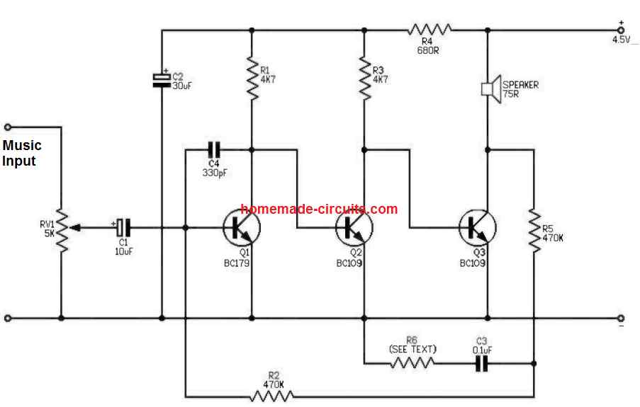
When power output, harmonic, distortion, frequency response are not considered critical for an amplifier, for example in small radios receivers, applying a class 'A' amplifier becomes a favorable choice. The circuit shown below makes use of just 3 transistors, is able to amplify with an output transformer, and provides an output power between 100 -200mW. It operates using a battery supply as low as 4.5V.
RV1 works like a volume control and hooks up with the amplifier stage by means of C1. The below discussed three stages are directly connected. The base bias of Q1 is implemented by resistors R2 and R5. Resistor R1 and transistor Q1 behave like a bias potential divider for Q2 base and likewise resistor R3 and transistor Q2 perform the bias base for the transistor Q3.
Resistor R2 and resistor R5 additionally work like a section of an overall negative feedback loop enhancing the frequency response of this BJT class A amplifier circuit, and also minimizing its distortion. A bargain between gain and quality is determined through appropriate selection of R6 and C3 values.
C3 is configured like a decoupling capacitor and R6 value can be found through some experimentation. (The lowest possible value of R6 should not be below 22k).
4) Class A Power Amplifier Circuit
The key benefit of a class A amplifiers is that is works without any crossover distortion. Alongside this significant advantage we find a big disadvantage of forever hot heatsinks and large wattage power supplies.

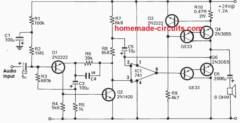
The circuit displayed above consists of a number of good features and is capable of providing a 5W of genuine class A audio into an 8 Ohm load. Q1 and Q2, in conjunction with the connected parts, work like a top-notch voltage amplifier with all round ac and dc feedback fed from the Q2 collector by means of R6 to the Q1 emitter.
The output stage genuinely includes Q6 and Q7 configured like an emitter follower Darlington pair. These transistors are driven by IC1, which is a 741 op amp. These BJTs can be also seen incorporated in the 741's feedback loop. These three elements together constitute a almost ideal output stage having an input impedance of many megohms along with a bandwidth ranging from a DC to higher than 100KHz.
Quiescent current is provided by The constant current source formed by the transistors Q3, Q4, Q5, R9 and R10 determine the quiscent current of the circuit. The utilization of a constant current source in this class A amplifier design appropriately isolates the output stage from supply line fluctuations and ripple.
Using the indicated part values, the circuit gets a a bandwidth between 10Hz - 30KHz -3db, with a distortion much lower than 0.1% just before clipping. The circuit also offers an input impedance of 1.5M and a sensitivity of 180mV for the complete output power.
Transistors Q4 to Q7 should be attached to an appropriate heatsink, which may have a dimension of 5" by 4" and should be finned type. These heatsinks should be installed vertically and positioned in such a way that it gets exposed to adequate air flow.
5) Another Good Class Amplifier Circuit

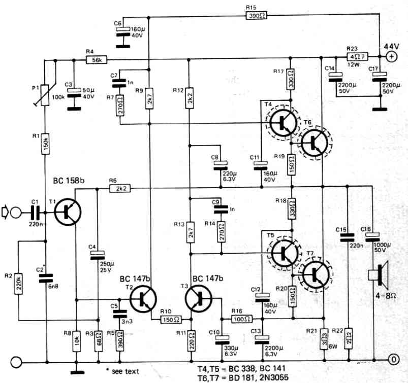
The problem with class A amplifier circuits is their reduced efficiency in comparison to class B stages. With this particular layout, and applying a 44 V power supply the quiescent current is going to be around 960 mA.
An output power of around 15 W is going to be supplied directly into an 8 Ohm loudspeaker. Harmonic distortion can be expected to be lower than 0.1%.
The input sensitivity of ths design can be around 360 mV for with respect to power output, this can be around 15 W into 8 Ohm speaker. The input impedance will be roughly 150 k.
For preamplifiers having a 1 k source impedance, capacitor C2 is going to be 6n8, for 2 k source impedance it will probably be 3n3. This class A amplifier provides a great feature of being short circuit proof; if you find a short it is going to consume roughly 1.6 A.
The potentiometer P10 is employed for implementing the offset control to the the no-signal output voltage at the intersection of the parts R18/R19 (around 21 V).
Every single output transistor (T6 and T7) must be mounted over a large heat sink, the thermal resistance must not be lower than 3.3°C/W; driver transistors T4 and T5 will necessitate a clip type heatsink.
6) 5 Watt Class A Amplifier Circuit
This class A amplifier circuit produces 5 watts rms into an 8 ohm load, however it needs a supply of 22 to 24 volts at 1 amp. This results in a maximum efficiency of around 19%, which is lower than 1/3 of the efficiency of typical Class B configurations.

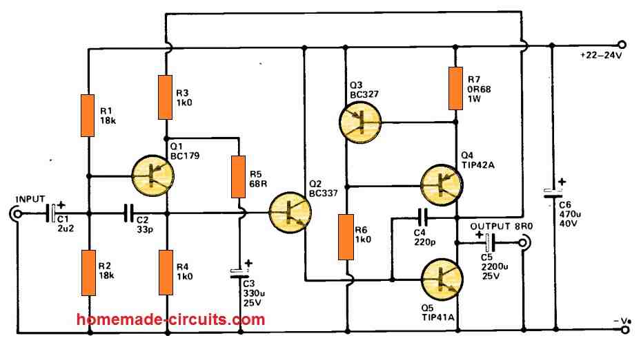
Q1 is utilized in the common emitter input stage and is linked directly to the output stage through the emitter follower buffer transistor, Q2. The latter is essential due to the output stage's rather large driving current. The output transistor, Q5, is used in common emitter mode. Its collector load is produced by Q3, Q4, and R7, and it is a constant current source. The latter fixes the circuit's output current to slightly below 1 amp.
The constant current generator load has a higher efficiency and linearity compared to an ordinary load resistor. At DC, R3 provides nearly 100 percent negative feedback to the amplifier, resulting in unity voltage gain. R1 and R2 bias the input to 1⁄2 the supply voltage, which likewise biases the output to the desired level of 1⁄2 the supply voltage.
At audio frequencies, R5 and C3 eliminates some of the feedback, allowing the circuit a maximum output sensitivity of around 380 mV rms. C1 and C5 enable DC blocking at the input and output, correspondingly, while C2 and C4 help with stability. Q4 and Q5 need to be placed atop a large heatsink.
Smallest Two Transistor Design
This simple two transistor class A amplifier circuit works by using Tr1 as a common emitter driver stage configured to directly operate Tr2; the common source output stage. R1 to R3 are positioned to bias the circuit to ensure that we have a quiescent current of approximately 25mA by means of LS1 and Tr2. The input signal modifies this current both side of the quiescent value, allowing the required operation of the loudspeaker LSI.

The output current swings through 0 to around 50mA at the peak output, and the typical current consumption as a result stays consistent at 25mA, and does not increase at higher output levels such as the case of a class B amplifier. The output power from this circuit is barely around 23mW RMS, nevertheless it is sufficient for several applications (tiny radios, intercoms, etc.).
The circuit provides fairly decent audio quality; the major constraint on the audio quality being the distortion levels, and restricted frequency response from the tiny high impedance loudspeaker employed. An input signal of merely around 80mV RMS is necessary to be able to generate a optimum output, however this value could be modified, to some extent, by adjusting the value of R5.
Alterations in the value of R5 leads to an inversely proportional variation in the input sensitivity of the circuit. A low impedance loudspeaker is not recommended in this circuit, since that might cause a high current to move via Tr2 and the loudspeaker, most likely leading to the break down of one of these or both.
Improving the above Design
The above circuit has a minor flaw due to the presence of a lingering current in the loudspeaker, causing the cone to never move back and forth around its usual resting position, but to constantly be offset one way or the other. The loudspeaker's performance may suffer as a result of this.
the following improved design eliminates the above issue.
