
When we talk about hot-swap controllers, it is basically an electronic device or integrated circuit (IC) that allows you to the insert or/and remove circuit boards, modules or parts within an active system without having you to switch off the system.
It regulates the surge current whenever a component is installed and protects from short circuits and overcurrent problems while the component is in use.
This enables the substitution of damaged components, enhancements, or maintenance without shutting down the whole system, that is critical for high-availability systems such as servers and network switches.
Overview
In hot-swap applications, the TPS2471x's primary function is to reliably drive an external N-channel MOSFET at 2.5 V to 18 V. Using fault timing and adjustable current limitations, it safeguards the supply and load from excessive current during startup.
Additionally the circuit guarantees that the external MOSFET stays inside its safe operating area (SOA). It controls inrush current as well. Moreover using this hot swap power supply you can now replace faulty parts of the load circuit without having to shut off the input power.
The TPS24710/11/12/13 is a type of controller that is easy for us to use. It is made to work with voltages from 2.5 V to 18 V and it is what they call a hot-swap controller and this means it is able to safely control an external N-channel MOSFET.
Also we can see that it has a programmable current limit and fault time and these are there to keep the supply and load safe from too much current when we are starting things up.
After the device starts up we let currents go above the limit that was picked by the user but only until a timeout that has been programmed happens. However if there are really big overload events we will immediately disconnect the load from the source.
The thing is the current sense threshold is low it is at 25mV and it is very accurate so we are able to use sense resistors that are smaller and work better which means there is less power lost and the footprint is smaller.
In addition the programmable power limiting makes sure the external MOSFET is always working inside its safe operating area SOA.
Because of this we are able to use MOSFETS that are smaller and the system ends up being more reliable. Also there are power good and fault outputs that we can make use of for keeping an eye on the status and controlling the load further down the line.
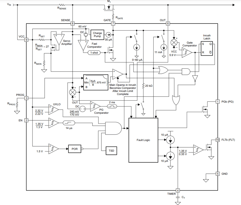
Functional Block Diagram
Pinout Details
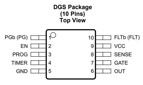
| NAME | PINS (TPS24710/11) | PINS (TPS24712/13) | I/O | DESCRIPTION |
|---|---|---|---|---|
| EN | 2 | 2 | I | Active-high logic input for enabling the device. Connects to a resistor divider. |
| FLT | – | 10 | O | Open-drain output (active-high) that signals an overload fault, causing the MOSFET to turn off. |
| FLTb | 10 | – | O | Open-drain output (active-low) that indicates an overload fault, turning off the MOSFET. |
| GATE | 7 | 7 | O | Output for driving the gate of an external MOSFET. |
| GND | 5 | 5 | – | Ground connection. |
| OUT | 6 | 6 | I | Monitors MOSFET power by sensing output voltage. |
| PG | – | 1 | O | Open-drain output (active-high) indicating power-good status, based on MOSFET voltage. |
| PGb | 1 | – | O | Open-drain output (active-low) that signals power-good status, determined by MOSFET voltage. |
| PROG | 3 | 3 | I | Sets the maximum power dissipation of the MOSFET by connecting a resistor from this pin to GND. |
| SENSE | 8 | 8 | I | Current sensing input for monitoring voltage across a shunt resistor between VCC and SENSE. |
| TIMER | 4 | 4 | I/O | Connects to a capacitor to define fault timing duration. |
| VCC | 9 | 9 | I | Supplies power and senses input voltage. |
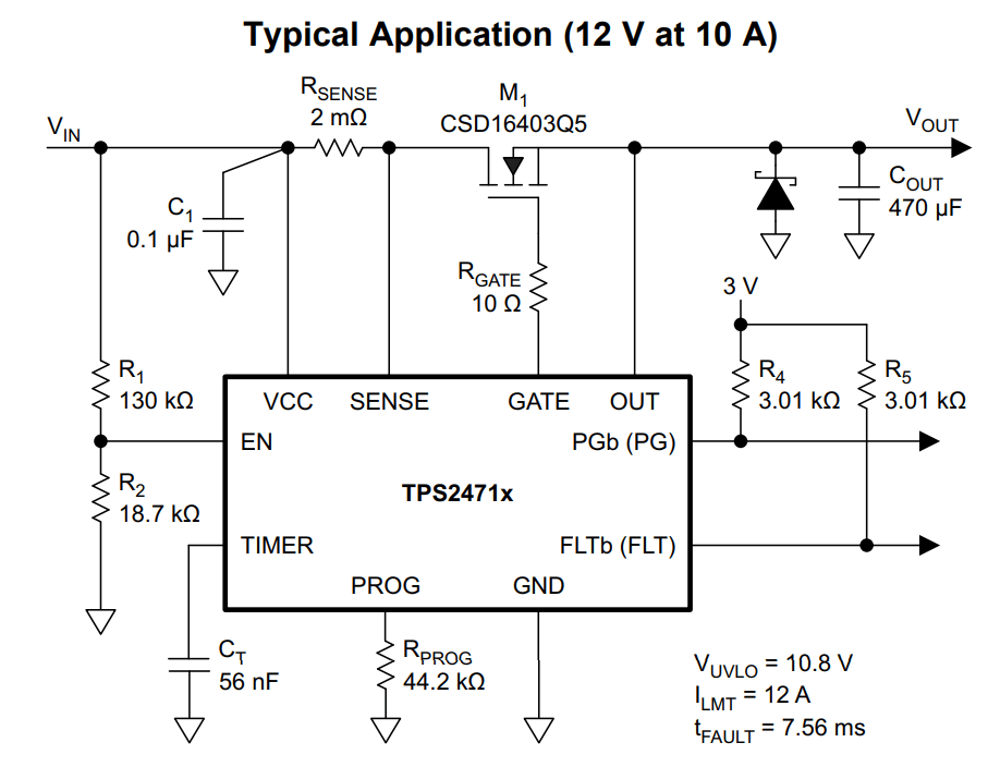
Circuit Diagram
Pin Description
EN
When we apply a voltage of 1.35 V or more to this particular EN pin it turns on or enables the switch for the gate driver.
If we add an external resistor divider it lets the EN pin act like an undervoltage monitor keeping an eye on the voltage levels.
Now if we cycle the EN pin by bringing it low and then back high it is like we are hitting the reset button for the TPS24710/11/12/13 especially if it has previously latched off because of a fault condition.
It is important that we do not leave this pin floating it needs to be connected to something.
FLT
The FLT pin is specifically for the TPS24712/13 variants. This active-high open-drain output goes into a high-impedance state when the TPS24712/13 has been working in current limit for too long causing the fault timer to expire.
How the FLT pin acts really depends on which version of the IC we are using. For the TPS24712 it works in latch mode. On the other hand the TPS24713 operates in retry mode.
When we are in latch mode if the fault timer runs out it turns off the external MOSFET and keeps the FLT pin in an open-drain condition. To reset this latched mode we can cycle either the EN pin or the VCC.
Now if we are in retry mode when the fault timer expires it first turns off the external MOSFET. Then it waits for sixteen cycles of the TIMER to charge and discharge.
After waiting it tries to restart. This whole process keeps repeating as long as the fault is still there. In retry mode the FLT pin becomes open-drain any time the fault timer disables the external MOSFET.
If we have a continuous fault the FLT waveform turns into a series of pulses. It is worth noting that the FLT pin does not activate if something else disables the external MOSFET like the EN pin an overtemperature shutdown or UVLO undervoltage lockout. If we are not using this pin we can leave it floating.
FLTb
The FLTb pin is specifically for the TPS24710/11. This active-low open-drain output goes low when the TPS24710/11/12/13 has been in current limit long enough for the fault timer to say "time is up".
How the FLTb pin behaves depends on the IC version we are using. The TPS24710 works in latch mode while the TPS24711 works in retry mode.
If we are in latch mode a fault timeout will turn off the external MOSFET and hold the FLTb pin low. To reset the latch mode we can cycle the EN or VCC. If we are in retry mode a fault timeout will first turn off the external MOSFET then wait for sixteen cycles of TIMER charging and discharging and then try to restart.
This whole process will repeat as long as the fault is present. In retry mode the FLTb pin is pulled low whenever the fault timer disables the external MOSFET.
If there is a continuous fault the FLTb waveform becomes a series of pulses. Keep in mind the FLTb pin does not activate if the external MOSFET is disabled by the EN an overtemperature shutdown or UVLO. If we are not using this pin it can be left floating.
GATE
The GATE pin is really important because it is how we drive the external MOSFET essentially telling it what to do. To help with this there is a charge pump that gives a current of 30 µA. This extra current helps the external MOSFET perform better.
To make sure the voltage between the gate and source does not go too high and cause damage there is a clamp set at 13.9 volts between the GATE and VCC. This is especially important because VCC is usually very close to VOUT when things are running normally.
When we are first starting up a transconductance amplifier carefully adjusts the gate voltage of a specific MOSFET (M1). This helps limit the inrush current which is a surge of current that can happen when you first turn something on.
During this time the TIMER pin is charging a timer capacitor (CT). This limiting of the inrush current continues until the voltage difference between the GATE and VCC goes over a certain point called the Timer Activation Voltage. This voltage is 5.9 volts when VCC is at 12 volts.
Once the voltage difference goes over this threshold the TPS24710/11/12/13 goes into what is called circuit-breaker mode.
The Timer Activation Voltage acts like a trigger once the voltage hits that point the inrush operation stops and the TIMER stops providing current and starts sinking it instead.
Now in circuit-breaker mode we are constantly watching the current going through RSENSE and comparing it to a limit based on the power-limit scheme of the MOSFET (check out PROG for more details on this).
If the current through RSENSE goes over this limit the MOSFET M1 will be switched off to protect it. The GATE pin can also be disabled in a few specific situations.
The GATE is pulled down by an 11-mA current source when certain fault conditions happen:
The fault timer runs out of time during an overload current fault (when VSENSE goes over 25 mV).
The voltage VEN drops below its set level.
The voltage VVCC goes below the under-voltage lockout (UVLO) threshold.
If there is a hard short circuit at the output the GATE is pulled down by a much stronger 1 A current source for a very short time (13.5 µs).
This only happens if the voltage difference between VCC and SENSE is more than 60 mV which tells us there is a fast-trip shutdown situation. After this quick shutdown an 11-mA current is used to keep the external MOSFET turned off.
Finally if the chip gets too hot exceeding the over-temperature shutdown threshold the GATE pin is also disabled. The GATE pin will stay low in latch mode for certain versions of the chip (TPS24710 and TPS24712). For other versions (TPS24711 and TPS24713) it will periodically try to restart.
One important thing to remember we should not connect any external resistor directly from the GATE pin to ground (GND) or from the GATE pin to the output (OUT).
GND
The GND pin is quite straightforward it is where we connect to the system's ground. Think of it as the common reference point for all the voltages in the circuit.
OUT
The OUT pin is really important for monitoring the voltage difference between the drain and source of the external MOSFET also known as M1. This voltage reading is necessary for both the power-good indicator (PG/PGb) and the power-limiting engine.
Both rely on accurate measurements from this pin to work properly. To protect the OUT pin from any potentially damaging negative voltage spikes we should use a clamping diode or enough capacitors.
For situations where there is a lot of power we suggest a Schottky diode rated at 3 A and 40 V in an SMC package as a good clamping solution.
We also need to bypass the OUT pin to GND using a low-impedance ceramic capacitor. The capacitance of this capacitor should be somewhere between 10 nF and 1 μF.
PG
The PG pin is specifically for the TPS24712/13 components. This output works in an active-high mode which means it goes high when things are good and is set up as an open-drain.
This makes it easy to connect to DC/DC converters or other monitoring circuits.
The PG pin goes into a high-impedance state which means it is essentially disconnected when the drain-to-source voltage of the FET goes below 170 mV. This happens after a short delay of 3.4 milliseconds to avoid false triggers. Conversely it will pull low when the VDS goes above 240 mV.
After the VDS of M1 increases the PG pin goes to a low-impedance state which means it is actively pulled low after the same 3.4-ms delay. This happens when the GATE is pulled to GND because of any of these situations:
We detect an overload current fault which means VSENSE is greater than 25 mV.
There is a severe short circuit at the output causing V(VCC – SENSE) to be greater than 60 mV indicating we have reached the fast-trip shutdown threshold.
The voltage at VEN drops below its set threshold.
The voltage at VVCC drops below the under-voltage lockout (UVLO) threshold.
The temperature of the die goes above the over-temperature shutdown (OTSD) threshold.
It is important to remember that if you do not plan to use the PG pin you can simply leave it unconnected. It will not affect the operation of the rest of the circuit.
PGb
We designate the PGb pin specifically for the TPS24710/11 device. This particular output, in its operation, works with an active low configuration, and we characterize it by its open drain design which we have specifically crafted so it can connect with those DC/DC converters or monitoring circuits that are downstream from it.
We see that the PGb signal makes a transition, moving to a low state once we observe that the drain to source voltage (VDS) of the field effect transistor (FET) drops to a level below 170 mV, this happens after we have a deglitch delay that lasts for 3.4 milliseconds.
On the other hand, it reverts back, going to an open drain state when the VDS goes above 240 mV. After we see the VDS of M1 increase, something that occurs when the GATE is pulled down to ground under any of the circumstances we will list below, the PGb then enters a state of high impedance after we have waited for that same 3.4 ms deglitch delay:
The IC detects an overload current fault when it see that the VSENSE voltage goes above 25 mV.
If the IC finds that there is a severe output short circuit present, it can tell because the V(VCC - SENSE) reading is greater than 60 mV, which tells us that the fast trip shutdown threshold has been breached.
Observe that the voltage VEN falls to a level below the threshold that has been designated for it.
The VCC voltage dips, going below the under voltage lockout (UVLO) threshold.
Notice that the die temperature rises, going above the over temperature shutdown (OTSD) threshold.
It is worth noting that we can leave this pin unconnected if we do not need to utilize it.
PROG Resistor
To regulate the maximum power that we allow in the external MOSFET M1 during those inrush conditions, we need to connect a programmable (PROG) resistor from this pin PGb to ground. It is crucial that we avoid applying any voltage to this pin.
If you do not need a constant power limit then you should employ a PROG resistor that has a value of 4.99 kΩ. To determine what the maximum power is, we can utilize the following equation(1):
RPROG = 3125 / (PLIM * RSENSE + 0.9 mV * VCC)
For the purpose of calculating the power limit based on an RPROG that already exists we should apply the following PLIM equation(2) which is the allowed power limit of MOSFET M1:
PLIM = 3125 / (RPROG * RSENSE) - (0.9 mV * V(VCC-OUT)) / RSENSE
In this formula RSENSE is the load current monitoring resistor that is connected between the VCC pin and the SENSE pin. Also, RPROG is the resistor that we connect from the PROG pin to GND.
We measure both RPROG and RSENSE in ohms, and we measure PLIM in watts. We determine PLIM by looking at the maximum allowed thermal stress of MOSFET M1 which we can find using another equation:
PLIM < (TJ(MAX) - TC(MAX)) / RΘJC(MAX)
In this equation, TJ(MAX) represents the maximum desired transient junction temperature and TC(MAX) is the maximum case temperature before we start or restart things.
Then RΘJC(MAX) stands for the junction to case thermal impedance of the pass MOSFET M1 and we measure it in units of °C/W. We measure both TJ(MAX) and TC(MAX) in °C.
SENSE
The SENSE pin is where we connect the negative terminal of RSENSE. This pin gives us a way of sensing the voltage across this resistor. It also gives us a way to monitor the drain to source voltage across that external FET. We set the current limit ILIM with this equation:
ILIM = 25 mV / RSENSE
We see a fast trip shutdown happen when V(VCC - VSENSE) goes above 60 mV.
TIMER
A capacitor CT which we connect from the TIMER pin to GND determines how the overload fault timing works.
The TIMER sources 10 µA when we have an overload present, and it discharges CT at 10 µA otherwise. M1 is turned off when VTIMER reaches 1.35 V.
If we are using auto retry after there is a fault then this capacitor also determines how long we wait before the external MOSFET is re enabled.
We recommend a minimum timing capacitance of 1 nF to be sure that the fault timer is operating properly. We can figure out the value of CT we need from the fault time we want which is tFLT, using this formula:
CT = (10 µA / 1.35 V) * tFLT
We find that the latch mode which applies to the TPS24710 and TPS24712 or the retry mode which applies to the TPS24711 and TPS24713 happens if the load current goes over the current limit threshold or the fast trip shutdown threshold.
While in latch mode the TIMER pin keeps charging and discharging the capacitor that is attached to it periodically, in retry mode the external MOSFET is disabled for sixteen cycles where the TIMER pin is charging and discharging.
At the end of that sixteenth cycle of charging and discharging the TIMER pin is pulled to GND by a 2 mA current source.
After that the external MOSFET is re enabled. We can also discharge the TIMER pin capacitor CT to GND during either the latch mode or the retry mode by using a 2 mA current source and this will occur whenever any of the following things happen:
VEN goes below its falling threshold
VVCC drops below the UVLO threshold
VCC
The VCC pin has three jobs that it performs for us. First it gives biasing power to the integrated circuit. Second it acts as an input to the power on reset which we call POR and the undervoltage lockout which we call UVLO functions.
The VCC trace that comes from the integrated circuit needs to connect right to the positive terminal of RSENSE so that we keep the voltage sensing error as small as possible.
The bypass capacitor C1 which you can see in a typical application diagram should be connected to the positive terminal of RSENSE. We recommend that, this capacitance should be at least a 10 nF capacitor.
Absolute Maximum Ratings
| Parameter | Conditions / Pins | Min | Max | Unit |
|---|---|---|---|---|
| Input Voltage Range | EN, FLT(2)(3), FLTb(2)(4), GATE, OUT, PG(2)(3), PGb(2)(4), SENSE, VCC | –0.3 | 30 | V |
| PROG(2) | –0.3 | 3.6 | V | |
| SENSE to VCC | –0.3 | 0.3 | V | |
| TIMER | –0.3 | 5 | V | |
| Sink Current | FLT, PG, FLTb, PGb | 5 | mA | |
| Source Current | PROG | Internally limited | mA | |
| Temperature | Maximum Junction, Tj | Internally limited | °C |
Notes:
- Exceeding these ratings may permanently damage the device. These are stress limits and do not indicate operational conditions.
- Do not apply voltages directly to these pins.
- Applicable to TPS24712/13.
- Applicable to TPS24710/11.
Recommended Operating Specifications for the IC
| Parameter | Conditions / Pins | Min | Nom | Max | Unit |
|---|---|---|---|---|---|
| Input Voltage Range | SENSE, VCC | 2.5 | 18 | V | |
| EN, FLT, FLTb, PG, PGb, OUT | 0 | 18 | V | ||
| Sink Current | FLT, FLTb, PG, PGb | 0 | 2 | mA | |
| Resistance | PROG | 4.99 | 500 | kΩ | |
| External Capacitance | TIMER | 1 | nF | ||
| Operating Junction Temperature Range | Tj | –40 | 125 | °C |
How the Hot-Swap Controller TPS24710/11/12/13 Works
Board When Powered
When we plug a hot swap board controlled by the TPS24710/11/12/13 into a system bus we primarily see the bypass capacitor charge current and small bias currents at first.
The TPS24710/11/12/13 stays inactive for a bit to stabilize its internal voltages. During this time the GATE PROG and TIMER pins are held low while the PG FLT PGb and FLTb pins are held open drain.
Once the voltage on the internal VCC rail goes above roughly 1.5 V the power on reset POR circuit starts up the TPS24710/11/12/13 and it is ready for a start up cycle. After the internal voltages stabilize and the external EN enable thresholds are met the GATE PROG TIMER PG FLT PGb and FLTb pins are released.
The device then starts sending current from the GATE pin to turn on the MOSFET M1. The TPS24710/11/12/13 keeps an eye on both the drain to source voltage across MOSFET M1 and the drain current flowing through it.
Using these measurements the TPS24710/11/12/13 regulates the drain current by managing the gate voltage. This ensures the power dissipated within the MOSFET does not go over the power limit set by the user. The current then goes up as the voltage across the MOSFET goes down until the current hits the current limit ILIM.
Inrush Current Control
After we have set up the TPS24710/11/12/13 chips properly like we talked about in the Board Plug-In part and the EN pin is active something cool happens the GATE pin gets enabled. This means the VGATE voltage starts to go up.
As VGATE increases it eventually reaches the point where the MOSFET M1 starts to turn on. When this happens current begins to flow into those big storage capacitors downstream. Now if this current gets too high exceeding the limit that the power limit engine has set things get interesting.
To keep everything safe a feedback loop kicks in and starts controlling the MOSFET's gate. This makes the current through the MOSFET increase in a controlled way.
This is super important because it not only limits the inrush current that charges the capacitance but also makes sure the MOSFET does not get too hot and bothered by limiting its power dissipation to safe levels. If you want a deeper dive into how this power limiting works we can check out the "Action of the Constant Power Engine" section.
Also when the Gate is enabled the TIMER pin begins to charge the timing capacitor CT with a current of approximately 10 μA. The TIMER pin continues to charge CT until V(GATE – VCC) reaches the timer activation voltage (5.9 V for VVCC = 12 V).
The TIMER then begins to discharge CT with a current of approximately 10 μA. This tells us that the inrush mode is all wrapped up. Now if the TIMER pin's voltage goes above 1.35 V before V(GATE – VCC) reaches the timer activation voltage the GATE pin is pulled to GND.
This makes the hot-swap circuit go into either latch mode (for TPS24710/12) or auto-retry mode (for TPS24711/13).
Once the inrush operation is done and dusted the power limit feature takes a break.
At this point the hotswap circuit turns into a circuit breaker. If the load current goes over the current limit threshold the TPS24710/11/12/13 will switch off the MOSFET M1 after a set fault timer period. This protects our circuit from overcurrent situations.
The Constant-Power Engine's Operations
We have programmed our hotswap controller circuit to limit power to 29.3 Watts using a resistor. When current starts flowing through the MOSFET we see 12V across it our input voltage VVCC is 12V.
Because of our constant-power engine a current of 2.44 Amps flows which we get by dividing 29.3 Watts by 12V.
Now this current changes depending on the drain to source voltage to keep the power dissipation at 29.3W. The constant-power engine does this by tweaking the reference signal going to the current limit amplifier.
If we look at the measurements of power dissipated within the MOSFET labeled FET PWR we will see it stays pretty constant during this operation. This ends when the current through the MOSFET hits the current limit ILIM.
We can think of this as a type of foldback limiting. But it is not like the usual linear kind. Instead it lets the power device work close to its maximum ability. This helps to make the start up faster and allows us to use a smaller MOSFET.
Fast Trip Circuit Breaker
These devices monitor the load current by measuring the voltage across a component called RSENSE. They have two different levels or thresholds they are watching for the current-limit threshold and the fast-trip threshold.
If something goes wrong with the load and the current through RSENSE goes higher than the current limit but not quite high enough to hit the fast-trip threshold something happens. A small current around 10 μA starts charging a capacitor CT.
If the voltage on this capacitor reaches 1.35 V the external MOSFET is switched off. Now the TPS24710 will latch off while the TPS24711 will try to restart. Either way the FLTb pin will signal that there is a fault.
During this time the overload staying between the current limit and fast-trip thresholds is allowed for a short period. This shutdown process is sometimes referred to as an electronic circuit breaker.
Now if there is a really big problem like a severe overload or a short circuit the fast-trip threshold kicks in. If the voltage across RSENSE goes above 60 mV the GATE pin quickly pulls the external MOSFET gate to ground with about 1 A of current.
This very fast shutdown might cause some disturbances in the system but you can add a small resistor between the GATE pin and the MOSFET gate to help control the turn-off current. The fast-trip circuit only keeps the MOSFET off for a few microseconds.
After that the TPS24710/11/12/13 turns back on slowly letting the current-limit feedback loop take control of M1's gate. Then the hot-swap circuit either goes into latch mode (TPS24710/12) or auto-retry mode (TPS24711/13).
Automatic Restart
As designers working with the TPS24711/13, we need to understand its auto-restart feature. Specifically, after a fault causes the external MOSFET M1 to shut down, the TPS24711/13 will automatically attempt to restart.
To manage this auto-restart process, the internal control circuits use a counter called CT to keep track of 16 cycles before trying to turn M1 back on. This cycle repeats as long as the fault is present.
The timer function operates with a 1:1 charge-to-discharge current ratio. In the first cycle, the TIMER pin voltage starts at 0 V and increases until it reaches an upper threshold of 1.35 V. Then it decreases to 0.35 V before the restart attempt. For the next 16 cycles, the lower threshold remains at 0.35 V.
This reduced duty cycle helps keep the average power dissipation low during a short circuit almost as low as during normal operation. Because of this, we usually do not need extra thermal management to handle a long-lasting output short.
PG, FLT, PGb, FLTb, and Timer Operations
Remember that PG is for TPS24712/13 and PGb is for TPS24710/11.
The open-drain PG/PGb output provides a deglitched end-of-inrush indication based on the voltage across MOSFET M1. This is useful because we do not want a downstream DC/DC converter to start while its input capacitor COUT is still charging.
About 3.4 ms after COUT is charged the PG pin goes to an active-high state or the PGb pin goes to an active-low state. This delay ensures that M1 is fully on and that any transient conditions in the power circuits have settled before the converter starts.
This is important because we do not want the downstream converter to draw a lot of current before the power-limiting mechanism allows the MOSFET to handle the maximum current which is set by the current limit ILIM. If we skip this step we might have problems starting the system.
The pull-up resistor on the PG/PGb pin in the diagrams is just for show. How we connect it to the converter will depend on the specific application.
The PG/PGb pin might indicate that the inrush is over before the MOSFET is completely enhanced. The capacitor downstream should be charged to almost its full voltage by then.
We need to make sure that the on-resistance of the MOSFET is low enough so that the voltage drop across it stays below the minimum power-good threshold of 170 mV.
Once the hot-swap circuit is running the PG pin can revert to a low-impedance state and the PGb pin can go to a high-impedance state if the voltage from drain to source on MOSFET M1 goes above its upper threshold of 240 mV. This is a warning signal to the downstream converters. This warning can occur because of a few things:
An overload fault occurs (VSENSE > 25 mV)
A hard output short circuit occurs leading to V(VCC – SENSE) greater than 60 mV i.e. the fast-trip shutdown threshold has been exceeded
VEN is below its falling threshold.
VVCC drops below the UVLO threshold.
The die temperature goes above the OTSD threshold.
Basically FLT and FLTb are outputs that tell us when something is up with the current. FLT is for TPS24712/13 and FLTb is for TPS24710/11. They let us know that the fault timer has run out because the load current went over the set limit but not so much that it tripped the fast-trip.
Think of it like this:
The Fault Timer Starts: When the current goes above the limit a small current (around 10 μA) begins charging an external capacitor (CT). This capacitor is connected to the TIMER pin.
Charging the Capacitor: The fault timer is basically the time it takes for this capacitor (CT) to charge from 0 V to a certain voltage 1.35 V.
Timer Expires: When the voltage on CT reaches 1.35 V the fault timer is done.
FLT/FLTb Signals: At this point FLT (for TPS24712/13) goes to a high state and FLTb (for TPS24710/11) goes to a low state. If this condition is not happening FLT stays in a low-impedance state and FLTb stays in a high-impedance state.
So to make the fault timer work we need that external capacitor CT hooked up between the TIMER pin and the GND pin. The time it takes for the timer to run out depends on how long it takes CT to charge up to 1.35 V.
The fault timer starts counting when one of these three situations occur:
- In the inrush mode we see that the TIMER plays a crucial role in managing current flow to the timer capacitor CT, right after we activate the MOSFET, labeled M1. As we initiate this process, current starts to flow from the timer capacitor CT when the voltage difference V(GATE−VCC) exceeds a pre-defined activation voltage for the timer. This procedure is elaborated upon in the Inrush Operation section of our documentation. If this voltage difference does not reach the required activation threshold before the TIMER itself reaches 1.35 V, we can expect that the TPS24710/11/12/13 will deactivate the external MOSFET M1. Once this MOSFET is turned off, we have two possible outcomes for the TIMER: it may enter latch mode (for TPS24710/12) or retry mode (for TPS24711/13).
- In scenarios where we encounter an overload fault we observe that the TIMER begins supplying current to the timer capacitor CT as soon as the load current exceeds our established current limits. When the voltage across the timer capacitor reaches its upper limit of 1.35 V, the TIMER starts drawing current from CT which results in grounding the GATE pin. After a predetermined duration of the fault timer we find that the TIMER may transition into either latch mode (TPS24710/12) or retry mode (TPS24711/13).
- Similarly in cases of an output short-circuit fault, we note that the TIMER sources current to CT when load current exceeds our programmed limits following a rapid shutdown of M1. Once again when the voltage of CT hits 1.35 V, the TIMER begins to sink current from CT and pulls the GATE pin to ground. After this, the fault timer period elapses, and we can expect that the TIMER may switch to latch mode (TPS24710/12) or retry mode (TPS24711/13). Importantly if during this fault timer period the fault current drops below our programmed limit it allows for a decrease in voltage across the TIMER thereby enabling the pass MOSFET to remain active.
If we observe that the fault current decreases and falls below the predetermined current limit during the interval defined by the fault timer then we will notice that the VTIMER will experience a reduction in its value allowing the pass MOSFET to remain enabled.
It is essential to understand that the operation of the TIMER can differ significantly depending on whether it is in latch mode (as seen in TPS24710/12) or retry mode (as indicated in TPS24711/13).
When the timer capacitor reaches the upper threshold voltage of 1.35 V we can expect the following behaviors:
In latch mode we find that the GATE pin stays in a low state. The TIMER pin will then proceed to periodically charge and discharge the connected capacitor. This process will continue until the TPS24710/12 is eventually turned off due to under-voltage lockout (UVLO) or when it is disabled through enable (EN).
In retry mode we observe that the TIMER will engage in charging and discharging the capacitor (CT) between a lower threshold of 0.35 V and an upper threshold of 1.35 V for a total of sixteen cycles. Once these sixteen cycles are over, then the TPS24711/13 will make an attempt to restart.
At the end of this 16th cycle we see that the TIMER pin connects to ground, after which it will increase from 0 V to 1.35 V during the first half-cycle where the GATE pin provides current.
This cycle will persist until either the overload fault is resolved or until the TPS24711/13 is disabled by UVLO or EN.
Overtemperature Shutdown
In the overtemperature shutdown feature that we find in the TPS24710/11/12/13. This useful circuit is built right into the device and its main job is to keep everything safe by shutting down the gate driver if the temperature of the die gets too high—specifically if it goes beyond around 140°C.
When we hit that overtemperature threshold we also see some changes with the FLT, PG, FLTb, and PGb pins. They all switch to what we call high-impedance states which basically means they are not actively driving any signals during this condition.
The good news is that once the die cools down by about 10°C we can get back to normal operation without any issues.
Start-Up of Hot-Swap Circuit by VCC or EN
when we connect or disconnect something from the system bus, we control it by turning on and off a special switch called a MOSFET M1.
The TPS24710/11/12/13 has two ways to turn on our MOSFET M1:
First if we make VVCC go higher than the UVLO upper threshold while EN is already above its upper threshold, it sends some current to the GATE pin. After a little bit of time (we call this the inrush period), the TPS24710/11/12/13 will fully turn on MOSFET M1.
The second way is if we make EN go above its upper threshold while VVCC is already higher than the UVLO upper threshold. Just like before, this also sends current to the GATE pin and after that inrush period, it will fully turn on MOSFET M1.
Now we can use the EN pin to start up the TPS24710/11/12/13 at a chosen input voltage called VVCC. If we want to disconnect the load from the system bus, the GATE pin will sink current and pull the gate of MOSFET M1 low.
There are several ways that we can turn off the MOSFET if needed:
If theres a condition like UVLO, EN being turned off, load current going over a limit, a hard short at the load or if it gets too hot (OTSD) then M1 can be disabled.
There are three main conditions that can pull down the GATE pin:
The GATE gets pulled down by an 11-mA current source when any of these things happen:
The fault timer runs out during an overload (which means VSENSE is greater than 25 mV).
VEN goes below its falling threshold.
VVCC drops below the UVLO threshold.
The GATE gets pulled down by a 1-A current source for just 13.5 microseconds when there’s a hard output short circuit and V(VCC – SENSE) is greater than 60 mV. This is called fast-trip shutdown! After thats done, an 11-mA sustaining current keeps our external MOSFET turned off.
Finally if the chip die temperature gets too high and goes over the OTSD rising threshold, a 20-kΩ resistor will discharge the GATE to ground.
Original Source:
https://www.ti.com/lit/ds/symlink/tps24712.pdf?ts=1739244653601&ref_url=https%253A%252F%252Fwww.ti.com%252Fproduct%252FTPS24712