In this post I have explained how IC 555 can be used for making 10 different types of monostable multivibrator circuits, such as one-shot type, debounce preventor, retriggerable type, touch switch monostable circuit and many more.
A monotsable multivibrator circuit is a configuration in which, a short momentary pulse at the input of the circuit causes a one-shot momentary pulse at the output which has a prolonged or an extended duration or extended ON time. This extended pulse output stays ON for a time interval which is determined by a resistor/capacitor network of the circuit.
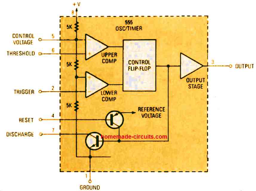
The image below shows the block diagram of the internal structure of the well-known 555 oscillator /timer, that is composed of a number of transistor stages which represent the upper and lower threshold comparators, a control RS flip-flop, and an output-amplifier stage.
The upper and lower thresholds of the comparators are internally fixed at 2/3rd and 1/3rd of the supply voltage using a resistive voltage-divider network

1) Standard Monostable Multivibrator
In the standard monostable mode, the THRESHOLD and DISCHARGE (pins 6 and 7) pinouts of the IC 555 are hooked up with each other and attached to the junction of a resistor and a capacitor configured like a RC network.
This RC configuration actually decides the output length of time of the IC's one-shot output. Figure 2 below displays a 555 constructed in the form of a one shot monostable timer.
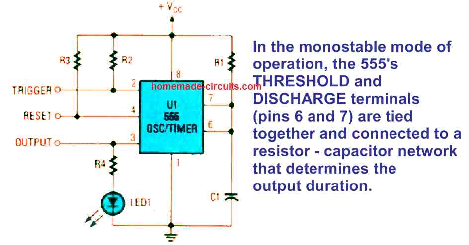
In this mode when the IC is switched ON by briefly connecting pin 2 with the ground line, the output of the IC at pin 3 instantly becomes high, and this high continues to hold for a period of time as fixed by the values of the resistor and the capacitor in the RC network connected at pins 6 and 7.
The timing count could be quickly aborted by temporarily grounding the pin 4 of the IC.
When the circuit is powered ON, the circuit initiates with a low at the output pin 3, and the capacitor of the RC network stays in the discharged condition through pin 7 of the 555.
As soon as a timing cycle is started by connecting pin2 to ground or the negative line C1 starts charging exponentially (via R1) towards the supply voltage level.
As soon as it gets to 2/3 voltage level of the supply, the IC 555 output pin3 becomes low yet again. This creates a shorting effect across C1, forcing the capacitor to discharge, which completes and finishes a single timing cycle for the IC.
The timing interval for which the output of the IC remains low does not depend on the supply voltage simply because the C1 charging level, and therefore the voltage introduced to the threshold input pin 6 of the IC, are both directly proportional to the supply voltage. The period of the time interval (T) can be expressed by the formula:
T= 1.1 x R1 x C1
Let's suppose R1 is selected to be a 1 megohm resistors and C1 is 1 uF, the output time for which the IC 555 output pin 3 would be low is: T =1.1 x 1,000,000 x .000,001= 1.1 seconds
The C1 value can be anywhere between 0.001uF to 100 µF; and R1 could be any value between 1k ohms and 10 megohms. It is advisable to have the capacitor C1 a low leakage type to guarantee improved timing accuracy.
As soon as the output of the 555 goes high due to a momentary ground signal at pin 2, applying further ground signal trigger pulses to pin 2 produces no effect on the output condition.
But, it may be possible to quickly abort the output ON time by applying a momentary ground or negative signal to pin 4 RESET pin of the IC. The action forces the 555's internal flip -flop to get reset, causing the 555's output to revert to low.
2) Another Basic Design
The next figure indicates the fundamental 555 monostable design. Usually the input of the monostable is configured to have a voltage level higher than 1/3rd of the supply voltage, and at the stand-by mode the IC 555's internal discharge transistor keeps C1 in an uncharged condition and the output at pin#3 stays low.
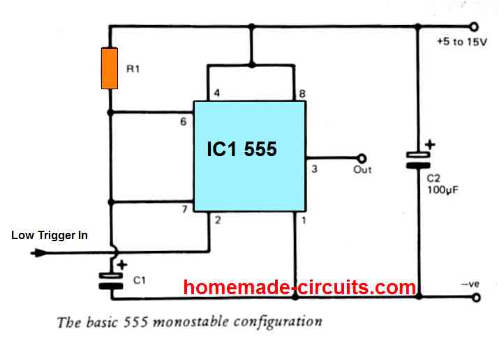
In case the trigger input is pulled lower than around 1/3rd supply voltage, causes the circuit is trigger ON, and the pin#3 of the 555 goes high. At this point the internal discharge transistor is turned off, which allows the capacitor C1 to begin charging through R1.
This carries on until the charge inside C1 gets to 2/3rd of the supply voltage, which then causes the monostable circuit to switch to its initial state. You can expect the circuit to revert to its original state only if the trigger input is allowed to return back to a level higher than 2/3rd of the supply voltage.
Until this situation is achieved, the output switch ON condition of the IC 555 persists and it does not quit. This is a crucial point that must be taken into account. The ON time of the output pulse at pin#3 is determined by the equation T = 1.1 CR seconds.
The least amount of pulse duration that could be achieved at pin#3 is approximately one microsecond, and the maximum pulse duration may be restricted simply with the highest amount of capacitance the timing capacitor C1 can offer.
However, this problem could be tackled by selecting a higher value for the resistor R2 so that it allows C2 discharge time to be longer.
This eventually restricts the chances of multiple bounces through which the circuit could be triggered.
The pulse trigger employed on pin#2 of the IC 555 can be hardly for a split second duration, and still the circuit should definitely work correctly, generating an output pulse that may be close to 10 us or higher.
For achieving shorter pulse lengths, for example a 1 us etc, you may want to to reduce the value of the timing capacitor C2, although this may result in unstable and inconsistent triggering, if C2 is made too low .
3) Monostable with Two Outputs
Figure 3 below indicates a 555 monostable having an additional output.
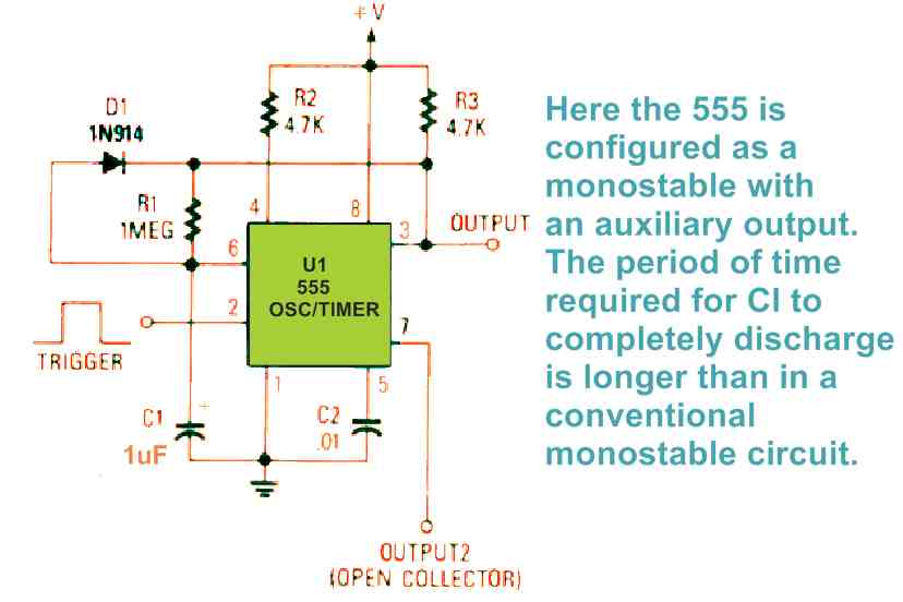
While the IC is in the quiescent or standby state, it output pin 3 stays low and the timing capacitor C1 (which is in effect connected in parallel with R1) remains discharged.
As soon as the circuit is triggered by a negative-going signal at pin 2, the output of the IC turns high, which causes the capacitor C1 to start charging via R1.
The moment the voltage across C1 gets to the stipulated upper limit level, the output reverts to low.
Due to this C1 begins discharging by means of D1 in the beginning, until the voltage drops to between 0.6 and 0.7 volt (the estimated voltage drop that exists across any silicon diode). When this occurs, C1 starts discharging the rest of its charge a lot more slowly by means of R1.
The length of time necessary for C1 to fully discharge will be higher compared to the normal monostable circuit (the main disadvantage of this type of circuit), and may result in timing issues and /or pulse-width variations when retriggered soon after the finish of a completed output pulse.
The circuit could be enabled by connecting a positive-going voltage (or pulse) with pin 4, or this can be halted simply by a applying ground voltage to pin 4.
In case a negative-going pulse is placed on the reset input of the 555, the timing cycle ends, and the action resets the output much earlier than the stipulated timing cycle is able to complete.
4) IC 555 Monostable with Push Button
One particular well-known undertaking while designing electronic circuits is to integrate switches or push buttons with the electronic circuit.
Since the associated standard switch bounce and noise can easily crank out many or intermittent output pulses, an intermediate buffer circuit (generally known as a "switch debouncer") is frequently utilized to get rid of these complications.
The following monostable circuit works great as an intermediate circuit to ensure the switch debounce is eliminated for the subsequent circuit associated with the pin3 of the monostable.
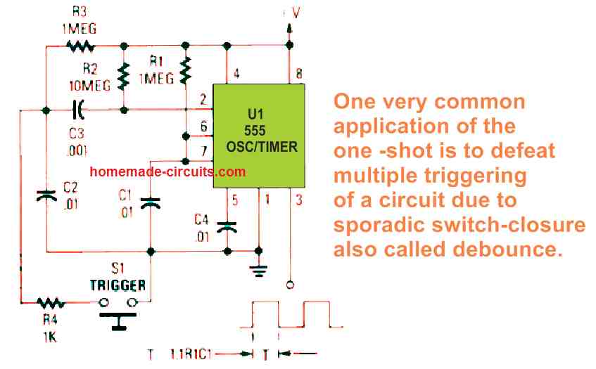
In the one-shot monostable circuit as demonstrated in the figure above, the 555 timer is triggered using a pushbutton S1. Just before the activation of S1, capacitor C1 is charged to the positive supply rail level through R1.
Next, the moment S1 is pressed, it causes C1 to discharge very fast by means of R4, which generates an instantaneous sharp negative surge voltage.
Any intermittent spikes happening due to the switch debounce on pressing S1, can be effectively eliminated due to the presence of R1 and C1, which enables a perfectly clean, negative-going spike.
This spike is subsequently allowed to move through C2 to pin 2 of 555 U1, triggering the monostable to activate, and generate a zero interference, clean square-wave output with a period of T= 1.1 x R1 x C1.
Then, as soon as the S1 is released, causes C1 to recharge to the +V potential level so that the circuit now goes in the standby mode, ready for the the next clean push button actuation cycle.
The monostable design allows a single fixed high output pulse when the S1 button is pressed, regardless of how long S1 is held depressed.
However the monostable circuit will be able to retrigger, as fast as S1 may allow to be reactuated. But it has to be ensured that the lowest possible output pulse duration of the design must be longer than the typical debounce period of the switch itself, mostly this should be around 10 ms or less.
5) Another Push Button Monostable
The next diagram illustrates an easy way of triggering a 555 monostable through a manual switching. However this approach is suited only in situations where an output pulse of a few seconds duration is acceptable.
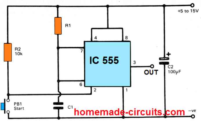
Push button PB1 has to be quickly released before the output pulse turns OFF, so that a correct working of the circuit is implemented.
This may not be the situation in case an output pulse of just a milliseconds is wanted, and most likely in this situation the pulse period is going to be equal to the of PB1 pressing time period, and not the intended time period that is set by the timing components R1 and C1.
6) Enhanced Push Button Triggering
An enhanced technique of manually triggered IC 555 monostable can be seen in the following figure.
In this design, the resistor R3 normally keeps the trigger input at practically the full positive supply level, but a short negative pulse is generated at the input as soon as push button PB1 is pressed, because pressing PB1 causes C2 to charge via R3.
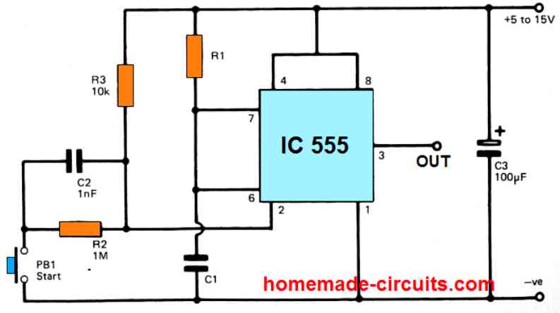
This provides the required short trigger pulse, and regardless of the time PB1 remains depressed, it is actually the R3 and C2 time constants that determines the final length of the output switch ON trigger pulse.
During the procedure, R2 discharges capacitor C2 quickly as soon as PB1 pressing is removed, which enables the circuit to be almost immediately prepared for the next PB1 pressed monostable operation.
One small difficulty that you may find with this enhanced push button monostable circuit is the multiple triggering of the circuit, which may be caused due to IC1 getting triggered during the periods PB1 push is released.
This may happen due to the mechanical contact bounce effect in the switch PB1.
7) Trimming the Monostable Output
It is also possible to tailor or reduce the pulse length of a 555 monostable output by applying a varying potential at pin#5 of the IC, which can be witnessed in the following figure.
If we increase the voltage at pin#5, also causes an increase in the threshold voltage of C1 which is responsible for determining the end time of the output pulse from its typical 2/3rd level. This as a result causes the output pulse to become longer.
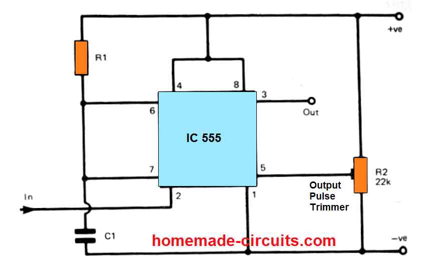
On the contrary if we reduce the pin#5 voltage, also causes a decrease in this threshold voltage which results in the shortening of the output pulse duration. This shown IC 555 monostable circuit provides an extremely large trimming range of approximately from -85% to +400%.
8) Touch Switch
A unique form of monostable circuit, configured like a touch switch can be witnessed in Fig. 5 below.
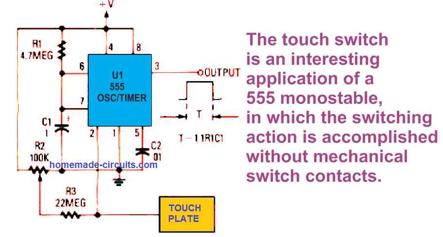
In this design, the switching function is achieved without involving any kind of traditional mechanized switch buttons. The circuit is essentially an old-fashioned 555 monostable, having just one key distinction, which is its style of triggering.
The resistor R1 is used for biasing the trigger input which helps to improve the sensitivity of the monostable circuit.
In this type of circuit, the trigger input requires very small amount of current during the time it remains above its 1/3 of the positive threshold. While using threshold control, resistor R2, is set to ensure the voltage at pin 2 is kept above 1/3 +V the monostable circuit output is held low until triggered.
As soon as the touch plate is contacted, the capacitance of the body (that now becomes effectively parallel with R3) causes the actual impedance between pin 2 and ground to drop. Due to this pin 2 potential is pulled below the 1/3 +V threshold.
This results in the triggering of the IC U1, causing an output pulse to genearte which has an ON time of T= 1.1 x R1 x C1.
It must be ensured that the set time period is longer than the average touch time on the touch plate. If this rule is not followed will result in the the timer getting retriggered even before the first timing pulse cycle is actually completed.
As indicated in the Fig. 5, the timing period of the monostable is approximately 5 seconds.
The touch plate could be any metal plate organized for easy finger touching. It may be also recommended to have some sort of feedback arranged such as an LED or buzzer, that will indicate the user regarding the successful touching and triggering of the circuit.
9) Retriggerable One-Shot Monostable
The circuit which is displayed in Fig. 6 is just one more version of the IC 555 monostable multivibrator, where we find the standard triggering features of the circuit has been changed.
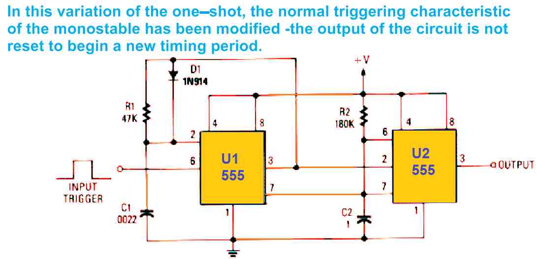
The circuit is different from the previous monostables since it works with a couple of IC 555's instead of one, Additionally, we do not have to reset the circuit to initiate a fresh timing cycle.
In this concept we can see the 555 timer U2 is wired like the normal monostable, and is triggered by a negative or ground pulse, supplied by 555 U1, which is hooked-up in the form of a basic inverting monostable.
The 555 U1's discharge pin 7 is wired to hold C2 for the time-span determined by the U1's output pulse period.
In the normal working conditions, when the trigger pulses tend to be longer than the time period U2, the output pulses appear with the rate of the input cycles, and the width of the output pulses corresponds to 1.1xR2xC2.
When the trigger pulses have shorter time duration than 1.1 x R2 x C2, the voltage across C2 is forced to come back to zero along with each pulse. As a result, C2 is never able to attain the 2/3 + V threshold as determined by the components R1/C2 for U2; which consequently causes U2 to never time out.
With the above conditions, the output of the circuit continues to be at a constant high DC level, and carries on in this way for so long as the input triggers are obtained with a time period lower than 1.1 x R2 x C2.
The Fig. 6 concept could be modified to work with just about any rate that corresponds with the appropriate selection of component values for 555.
The IC U1 555's output pulse-width of must be maintained at a certain modest percentage to that of IC 555 U2, ensuring that the pulse-width are sufficiently long and are able to satisfy the full discharge of C2 during the 555 U1's timing period.
10) Monostable Controlled with Light
The next diagram exhibits a 555 monostable multi-vibrator merged with a couple of light-controlled comparators to configure a circuit which you can use to activate the front door lights of your home for a some fixed period of time, and during the end of this time interval the light is turned off.
Remember that pin 7 of U1b is hooked up with pin 4 (reset) of U2. This is because we know that to ensure that a timing cycle gets initiated, pin 4 has to be held high.
If pin 4 were to be held low during the time a negative-going trigger pulse is given to pin 2 of the 555, no timing cycle would be initiated.
We also know that the LDR's possess a resistance of around 0.5 megohm in the absence of light and around 100 ohms with optimal light conditions.
When it is daytime the LDR R5 receives optimal amount of light, which causes its resistance to drop at around 100 ohms.
Since the resistance of R6 is much higher compared to the resistance of the LDR during daytime, it causes a far higher voltage to drop across R6, approximately to 5 V, while the drop across R5 is only 0.02V
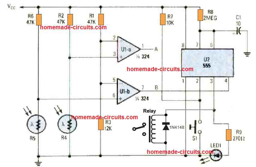
At this point, with the values the ersistors R1 and R3 have, less than 50 percent of the supply voltage, which is around 1.02 volt, reaches the inverting input of U1b.
With the op amp inverting input of U1b having a increased voltage difference than the non-inverting input, the U1 op amp output becomes low.
This low output reaches the pin 4 (reset) of U2, disabling the IC 555 function, which mens the implemtation of a negative or ground trigger pulse fails to reach the at pin 2 which keeps the initialization of the monostable switching cycle disabled.
But as the sun goes down, the R5 resistance goes higher and touches the maximum value of approximately 0.5 megohm. Due to this increase in the R5 resistance, the voltage drop across it as well raises, causing the U1b output to get less negative.
As soon as the R5 resistance goes over the 47k limit, the U1b output instantly turns positive, eliminating the disabling signal utilized to pin 4 of IC 555 U2.
Pushing S1 in this situation can trigger ON the IC 555 monostable timing cycle, causing pin 3 of U2 to go high, and switch ON any device connected to pin3 of the monostable IC 555.
For example a relay could be connected across pin3 and ground, and the N/O contacts of the relay wired across a series lamp and AC mains supply, which would cause the lamp to light up in this scenario, and remain illuminated as long as the monostable cycle keeps the relay ON.
Hello Sir. I’ve tried the 555 monostable on a breadboard and it works…but when soldering it on a PCB it doesn’t. I have done and re_done to no avail…What might be the problem please Sir?
Hello Jedidiah,
A 555 monostable circuit is a very basic circuit and I have built it number of times roughly on perfboards, without any care or precautions, and yet it always worked for me.
So, there must be some wrong connection in your PCB which might be causing the issue…only you can find it.
555 Timer Circuit with Modified Trigger Behavior
Requirements:
Timer starts on trigger rising edge.
Timer stops at 4sec if trigger is released within 4sec.
Timer stops if trigger is held beyond 4sec.
What does “timer stops” means in the following sentence, please elaborate?
Timer stops if trigger is held beyond 4sec.
I SENT THE SCHEMATIC TO HITMAN EMAIL
Hi Norman, I saw the diagram, however, sorry, i could not understand and simulate the retriggerable oscillations that you are facing in the circuit.
Hi Swagatam, I am using one of your electret mic relay circuits (the one with two npns and one pnp) and am using it to trigger a 555 one shot. The one shot triggers a cd4060. I would like the one shot to be retriggerable so it will extend the timeout time if the mic continues to receive sound. I found a 555 retriggerable one shot on the net that uses a transistor to short the timing capacitor to allow the 555 pin 3 to remain high while the cap is discharged. The cap then begins charging to continue the timing cycle. The problem is when I connect the output of the mic circuit to the transistor to short the capacitor, the mic circuit oscillates. The circuit works fine when not connected to the transistor that shorts the cap. What do you think I am doing wrong?
Hi Norman,
I have to see the schematic to understand its working. You can send the link of the article without the https.
By the way the 3 transistor/MIC circuit which you are referring to, itself has a very good monostable feature.
The monostable timing can be adjusted by tweaking the C2 capacitor value.
HI Swagatam, What is the value of c2 of the retriggerable one-shot circuit? Is C1 value 0.0022uF or 0.022uF. What would be a good minimum and maximum frequency of the input trigger?
Hi Norman,
C2 value should be a 0.1uF
C1 is 0.0022uF.
I am not sure what should be the min/max triggering frequencies, it will need to be calculated using formulas.
If possible I will try to figure it out.
Hello Eng. Thank you very much for the help and prompt response, I have been working in electronics for 20 years and since 2004 I have been chatting. But I tell you the truth, it’s a page like NONE, successes…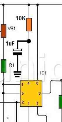
I added the 10k resistor and the 1uf capacitor as indicated…
" rel="ugc">
But I still have the problem of automatic activation of the 1st or 2nd sometimes the 3 relays when feeding with 12V., the circuit works fine,, Charge, Wash, Drain and return to the same thing, the shutdown is at my will then I will add one for a certain short and long time…
I only have to eliminate that activation by connecting to 12 vol dc
Thank you Felix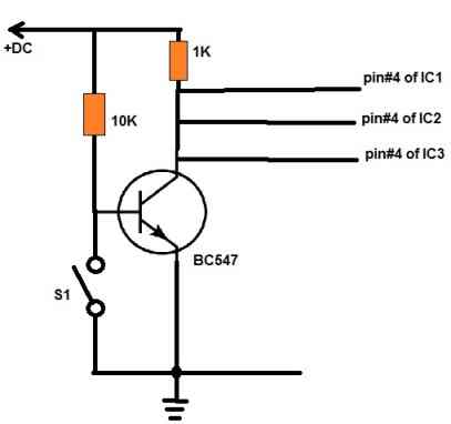
I will be glad if your problem is solved.
I am quite sure that the problem is happening due to improper resetting of the 555 ICs.
You can try the following modification and check how it works:
" rel="ugc">
Initially keep S1 switched OFF.
First switch ON the power supply to the circuit and then switch ON S1….please check how the circuit responds to this.
ok Ing, I’ll do that, but it’s taking out the previous change that you suggested,? the R10k with a 1uf capacitor on pin 4, or do I leave it included…??
If…S1 is off, it is my push button normally open..
– So I would have an independent key for when I power the circuit I have to reset.? and then press the other ground button and pin 2 of the 1st 555,, to start the wash.
Could you put a double button..? I mean 1 button to start and the other to reset.
IMPORTANT:…You could write me all your email, because the one you sent tells me that it does not exist, something is not correct.
Hello Felix,
I can understand you were trying send me the initial comment repeatedly, but as you can see I have already answered to your initial comment long back, so adding the same comment repeatedly was not a good idea that is why I had to delete your repeat comments.
To add the new modification you must remove the previous modification of 1uF and the 10K resistor on pin#4 of the IC.
Yes, so now you have an independent key to reset all the 555 ICs with a single push of the SPDT switch.
Double button is actually not required, this single switch will do both the jobs. It will reset all the ICs and also start (enable) the ICs
I actually prefer discussing through this comment platform because it allows sharing the discussions with all the other readers also.
ING what would be your email,,, to send you a livewire circuit to see,,, it works well but,,
Hello Felix,
I do not use softwares to simulate circuits, I always prefer building them practically to test them, so understanding a simulator result may not be possible for me.
Ing..este seria como hice…" rel="ugc">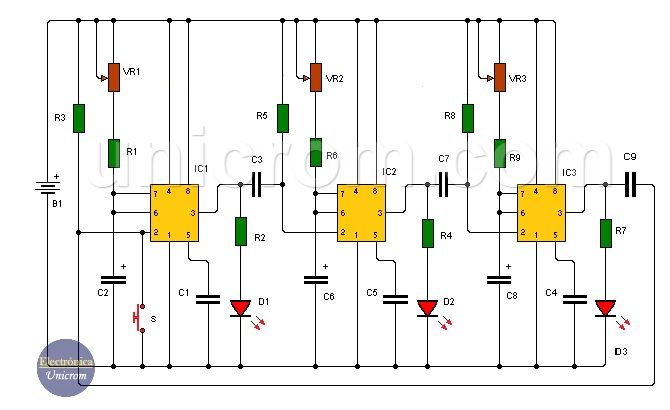
cuando alimento con 12V aveces prende todos los u aveces el 1er y 3er ,,Por QUE..?
antirrebote no creo,, por que sin dar el pulso para iniciar.
en los pinos 3 de los 555 tienen relay de 12V con diodos 1n 4148 mas el led indicador para saber que relay esta activo..
No problem, just add the following modification to each of the 555 ICs:
" rel="ugc">
Ing,,, I made a cascade circuit with three (3) 555 timing to my need… for a washing machine that I could not get the adjustment clock,, I made the circuit, everything works through a relay for each 555… timed,,The first 555 has a button to start the sequence.
12V power supply through the 7812.
The (1)..1st 555 enables the valve for water loading.
The (2)….2nd 555 enables the motor for the wash spin.
The (3)..3rd 555 enables the drain motor, then follows the sequence 1,2,3…1,2,3,,,1,2,3 then I’ll put another one for shutdown at a certain time.
PROBLEM: When turning on or feeding with 12Vdc, they are all activated together and sometimes 1 with 3… then only 1 remains, it completes its time, and goes to 2,3…1.2.3,,1,2,3 without problems .. BECAUSE…? If I put an ANTI-REBOUND … what would it do me, if I don’t hit the button.
I even started in a LIVEWIRE simulator that when feeding it already predicted that this would happen… HOW DO I SOLVE…???
Hi Felix,
OK, I guess you want to add a switch-ON reset facility to each of the 555 ICs
You simply have to do the following modification to each of your 555 ICs in the cascaded circuit:
" rel="ugc">
Eng… the 555 in cascade works well, I don’t know if you understood me correctly, they are 3 units of the 555… my problem is that by giving it 12 vol Dc, when powering the circuit it already enables relay 1 with 2 .after a time as if he had given it a pulse, that is, the order to start,,, a pulse and the sequence continues..
I have understood your problem correctly. You need to auto-reset each of the ICs at power switch ON. Please see the modification which needs to be done at pin#4 of the ICs.
Sir,
I may be totally off track, since I am just an enthusiast. My question however is can I combine the following: RETRIGGABLE ONE-SHOT MONOSTABLE CIRCUIT, 4017IC to form a 3 speed dc motor controller. If so can you direct me with a circuit diagram to facilitate same.
The block diagram of my idea is [RETRIGGABLE ONE-SHOT MONOSTABLE]-[4017 IC]-[12v DC MOTOR]
I will appreciate your response.
Best regards chaly.
Charles, the output of the retriggerable monostable will be always ON as long a retriggering is maintained at the input side. So how can this constantly ON output of this circuit can be used with a 4017 to form a 3 speed DC controller? I can’t figure it out.
Hi swagatam, I liked the idea of the lights control at sundown, but I have one issue, what happens if power fails ? The circuit will again switch on and remain for the same amount of time again. So if we have a power stop and resume at almost the end of the time cylce, won’t the lights remain ON again? Is there any modifications that could be done so that the lights remain ON only for the calculated period irrespective of power failure?
Hi Richard, unfortunately there’s no easy way to create a memory for the circuit. The possible way is to use a small battery so that it powers the circuit only, and the relay section is driven separately through a transistor driver and the power supply.
Thank you swagatam for your quick reply. I ll try that
You are welcome Richard!