In this section we are going to analyze BJT common-base configuration, and learn regarding its driving point characteristics, reverse saturation current, base to emitter voltage and evaluate the parameters through a practical solved example. In the later parts we will also analyze how to configure a common-base amplifier circuit
Introduction
The symbols and annotations utilized for representing transistor common base configuration in most of
the books and guides printed these days can be witnessed in the below shown Fig. 3.6 This may be true for both pnp and npn transistors.
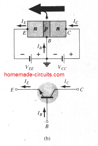
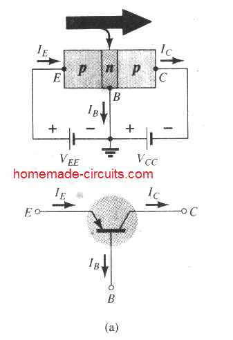
Figure 3.6
3.4 What is Common-Base Configuration
The term "common-base" arises from the fact that here the base is common to both the input and output stages of the arrangement.
Furthermore, the base typically becomes the terminal nearest to, or at, ground potential.
Throughout our conversation here, all current (Ampere) directions will be taken with respect to the conventional (hole) direction of flow and not the electron flow direction.
This selection has been decided chiefly with the concern that the large amount of document offered at academic and commercial organizations implements conventional flow, and the arrows in every electronic representations possess a path identified with this specific convention.
For any bipolar transistor:
The arrow mark in the graphical symbol describes the direction of flow of the emitter current (conventional flow) across the transistor.
Each of the current (Amp) directions showing up in Fig. 3.6 are the genuine directions as characterized by the selection of conventional flow. Observe in each case that IE = IC + IB.
Notice additionally that the biasing (voltage sources) implemented are specifically to ascertain current in the direction that's specified for each of the channels. Meaning, compare the direction of IE with the polarity or VEE for each configuration, and also compare the direction of IC with the polarity of VCC.
To comprehensively illustrate the actions of a three-terminal unit, for example the common-base amplifiers in Fig. 3.6, demands 2 sets of properties - one for the driving point or input factors and the other for the output section.
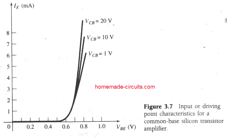
The input set for the common-base amplifier as displayed in Fig. 3.7 applies an input current (IE) to an input
voltage (VBE) for a variety of ranges of output voltage (VCB).
The output set applies an output current (IC) for an output voltage (VCB) for a variety of ranges of input current (IE) as demonstrated in Fig. 3.8. The output, or the group of collector characteristics, possesses 3 fundamental elements of interest, as pointed out in Fig. 3.8: the active, cutoff, and saturation regions. The active region will be the region typically useful for linear (undistorted) amplifiers. Specifically:
Within the active region the collector-base junction will be reverse-biased, while the base-emitter junction is forward-biased.
The active region is characterized by the biasing configurations as indicated in Fig. 3.6. On the lower end of the active region the emitter current (IE) will be zero, the collector current is in this situation simply as a result of reverse saturation current ICO, as illustrated in Fig. 3.8.
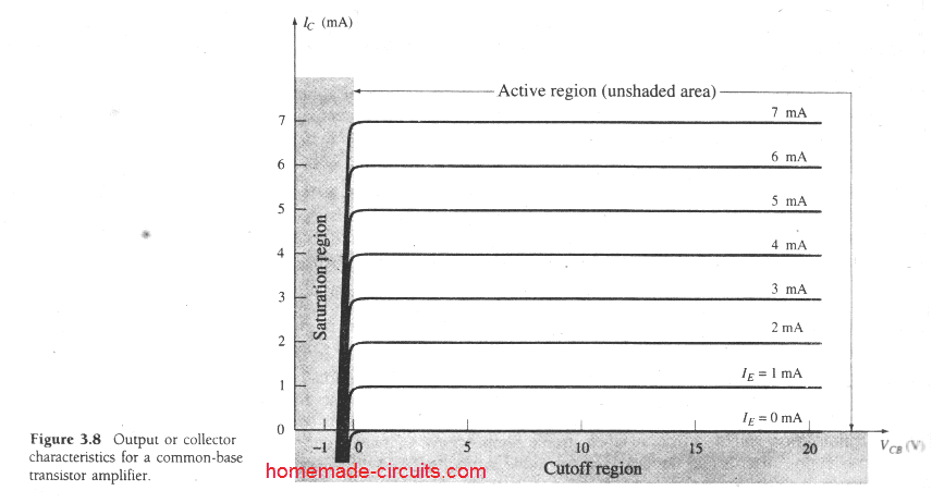
The current ICO is so negligible (microamperes) in dimension in comparison to the vertical scale of IC (milliamperes) that it presents itself practically on the same horizontal line as IC = 0.
The circuit considerations which are present when IE = 0 for the common-base setup can be seen in Fig. 3.9. The annotation most often applied for ICO on datasheets and spec sheets is as pointed out in Fig. 3.9, ICBO. On account of superior design methods, the degree of ICBO for general-purpose transistors (particularly silicon) within the low- and midpower ranges is normally so minimal that its influence could be overlooked.
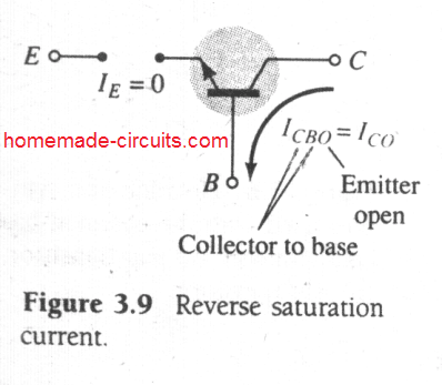
Having said that, for larger power devices ICBO might continue to show up in the microampere range. Furthermore, remember that ICBO, just like Is in case of diodes (both are reverse leakage currents) could be vulnerable to changes in temperature.
At increased temperatures the impact of ICBO may result being a crucial aspect because it can rise significantly quickly in response to temperature elevations.
Be aware in Fig. 3.8 as the emitter current rises over zero, the collector current goes up to a level primarily equivalent to that of the emitter current as established by the fundamental transistor-current relationships.
Notice also that there's quite an ineffective influence of VCB on the collector current for the active region. The curved shapes evidently reveal that an initial estimation to the relationship between IE and IC in the active region can be presented as:

As deduced from its title itself, the cutoff region is understood to be that location where the collector current is 0 A, as disclosed on Fig. 3.8. Furthermore:
In the cut-off region the collector-base and base-emitter junctions of a transistor tend to be in the reverse-biased mode.
The saturation region is identified as that section of the characteristics across the left side of VCB = 0 V. The horizontal scale in this area has been enlarged to distinctly reveal the remarkable enhancements made on attributes in this region. Observe the exponential upsurge in collector current in response to the increase in the voltage VCB toward 0 V.
The collector-base and base-emitter junctions can be seen to be forward-bias In the saturation region.
The input characteristics of Fig. 3.7 show you that for any predetermined magnitudes of collector voltage (VCB), the emitter current increases in such a way that may strongly resemble to that of the diode characteristics.
Actually, the effect of a rising VCB tends to be so minimal on the characteristics that for any preliminary evaluation the difference caused by variations in VCB could be disregarded and the characteristics could be actually represented as demonstrated in Fig. 3.10a below.
If we therefore utilize the piecewise-linear technique, this will produce the characteristics as revealed in Fig. 3.10b.
Taking this one level up, and disregarding the slope of the curve and consequently the resistance generated due to a forward-biased junction will lead to the characteristics as displayed in Fig. 3.10c.
For all the future investigations that would be discussed in this website, the equivalent design of Fig. 3.10c is going to be exercised for all dc evaluations of transistor circuits. Meaning , whenever a BJT is in the “conducting” status, the base-to-emitter voltage is going to be considered as expressed in the following equation: VBE = 0.7 V (3.4).

To put it differently, the influence of the changes in the value of VCB along with the input characteristics slope will tend to be overlooked as we make an effort to evaluate BJT configurations in such a way that may help us to acquire an optimal approximation towards the actual response, without too much involving ourselves with parameter which may be of less significance.
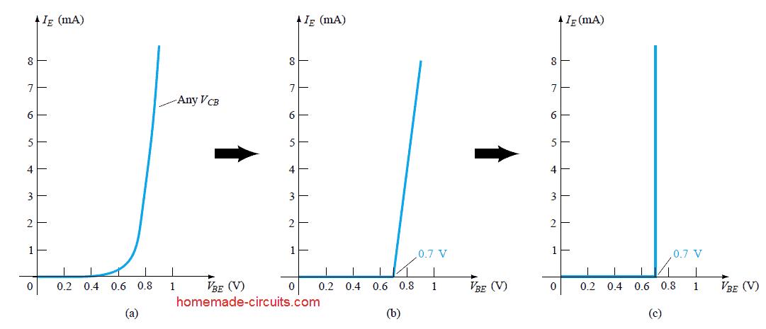
We all should actually thoroughly appreciate the assertion expressed in the above characteristics of Fig. 3.10c. They define that with the transistor in the “on” or active condition the voltage moving from base to emitter is going to be 0.7 V for any amount of emitter current as regulated by the associated external circuit network.
To be more precise , for any initial experimentation with a BJT circuit in the dc configuration, the user can now quickly define that the voltage through base to emitter is 0.7 V while the device is in the active region - this can be considered as an extremely crucial bottom line for all our dc analysis which would be discussed in our upcoming articles..
Solving a Practical Example (3.1)
In the above sections I have explained what is common-base configuration about the relationship between base current IC and emitter current IE of a BJT in section 3.4. With reference to this article we can now design a configuration which would allow the BJT to amplify current, as represented in Fig 3.12 below common-base amplifier circuit.
But before investigating this, it would be important for us to learn what is alpha(α).
Alpha(α)
In a common-base BJT configuration in the dc mode, due to the effect of the majority carriers, the current IC and IE form a relationship expressed by the quantity alpha, and presented as:
α dc = IC / IE -------------------- (3.5)
where IC and IE are the current levels at the point of operation. Although the above characteristic identifies that α = 1, in real devices and experiments this quantity could lie anywhere around 0.9 to 0.99, and in most cases this would be approaching towards the maximum value of the range.
Due to the fact that here alpha is specifically defined for the majority carriers, the Eq 3.2 which we had learned in the previous chapters now can be written as:

Referring to the characteristic in graph Fig 3.8, when IE = 0 mA, IC value consequently becomes = ICBO.
However, from our previous discussions we know that the level of ICBO is often minimal, and therefore it becomes almost unidentifiable in the graph of 3.8.
Meaning, whenever IE = 0 mA in the above mentioned graph, IC also turns into 0 mA for the VCB range of values.
When we consider an ac signal, wherein the point of operation travels over the characteristic curve, an ac alpha can be written as:

There are a few formal names given to ac alpha which are: common-base, amplification factor, short-circuit. The reasons for these names will get more apparent in the upcoming chapters while evaluating equivalent circuits of BJTs.
At this point we can find that Eq 3.7 above confirms that a relatively modest variation in the collector current gets divided by the resultant change in IE, while the collector-to-base is at a constant magnitude.
In majority conditions, the quantity of α ac and α dc are almost equal allowing an exchange of magnitudes among each other.
Common-Base Amplifier
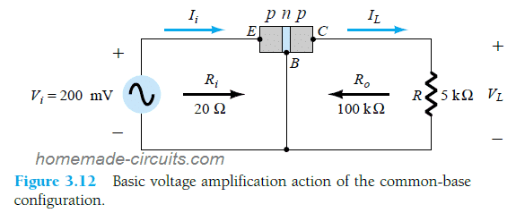
The dc biasing is not shown in the above figure since our actual intent is to analyze the ac response only.
As I have explained in our earlier posts regarding common-base configuration, the input ac resistance as indicated in Fig 3.7 looks quite minimal and varying typically within a range of 10 and 100 ohm. While in the same chapter we also saw in Fig 3.8 the output resistance in a common-base network looks significantly high, which could vary typically in the range of 50 k to 1 M Ohm.
These differences in resistance values is basically on account of the forward-biased junction appearing on the input side (between base to emitter), and the reverse biased junction appearing at the output side between base and collector.
By applying a typical value of say 20 Ohms (as given in the above figure) for the input resistance, and 200mV for input voltage, we can evaluate the amplification level or range at the output side through the following solved example:
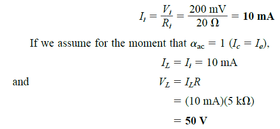
Thus, the voltage amplification at the output can be found by solving the following equation:

This is a typical voltage amplification value for any common-base BJT circuit which could possibly vary between 50 and 300. For such network, the current amplification IC / IE is always less than 1, since IC = alphaIE, and alpha is always less than 1.
In preliminary experiments the fundamental amplifying action was introduced through a transfer of current I across a low to a high-resistance circuit.
The relationship between the two italic phrases in the above sentence actually resulted in the term transistor:
transfer + resistor = transistor.
In the next tutorial I will elucidate Common-Emitter Amplifier
Reference: https://en.wikipedia.org/wiki/Common_base