

In this article I have explained the pinout functions of the IC SG3525 which is a regulating pulse width modulator IC. So I have explained in details:
Main Technical Features
The main features of the IC SG3525 may be understood with the following points:
- Operating voltage = 8 to 35V
- Error amp reference voltage internally regulated to 5.1V
- Oscillator frequency is variable through an external resistor within the range of 100Hz to 500 kHz.
- Facilitates a separate oscillator sync pinout.
- Dead time control is also variable as per intended specs.
- Has an internal soft start feature
- Shut down facility features a pulse by pulse shutdown enhancement.
- Input under voltage shut down feature also is included.
- PWM pulses are controlled through latching for inhibiting multiple pulse outputs or generation.
- Output supports a dual totem pole driver configuration.
Pinout Diagram of the IC

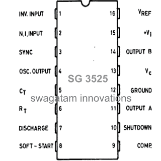

SG3525 PinOut Description
A practical implementation of the following pinout data may be understood through this inverter circuit
The IC SG3525 is a single package multi function PWM generator IC, the main operations of the respective pin outs are explained with the following points:
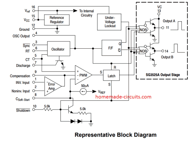
Pin#1 and #2 (EA inputs): These are inputs of the built-in error amplifier of the IC. Pin#1 is the inverting input while pin#2 is the complementary non-inverting input.
It's a simple op amp arrangement inside the IC which controls the PWM of the IC outputs at Pin#11 and Pin#14. Thus these EA pins 1 and 2 can be effectively configured for implementing an automatic the output voltage correction of a converter.
It is usually done by applying a feedback voltage from the output through a voltage divider network to the non-inverting input of the op amp (pin#1).
The feedback voltage should be adjusted to be just below the internal reference voltage value (5.1 V) when the output is normal.
Now, if the output voltage tends to increase above this set limit, the feedback voltage would also increase proportionately and at some point exceed the reference limit. This will prompt the IC to take necessary corrective measures by adjusting the output PWM, so that the voltage is restricted to the normal level.
Pin#3 (Sync): This pinout can be used for synchronizing the IC with an external oscillator frequency. This is generally done when more than a single IC is used and requires to be controlled with a common oscillator frequency.
Pin#4 (Osc. Out): It's the oscillator output of the IC, the frequency of the IC may be confirmed at this pin out.
Pin#5 and #6 (Ct, Rt): These are termed CT, RT respectively. Basically these pinouts are connected with an external resistor and a capacitor for setting up the frequency of the inbuilt oscillator stage or circuit. Ct must be attached with a calculated capacitor while the Rt pin with a resistor for optimizing the frequency of the IC.
The formula for calculating the frequency of IC SG3525 with respect to RT and CT is given below:
f = 1 / Ct(0.7RT + 3RD)
- Where, f = Frequency (in Hertz)
- CT = Timing Capacitor at pin#5 (in Farads)
- RT = Timing Resistor at pin#6 (in Ohms)
- RD = Deadtime resistor connected between pin#5 and pin#7 (in Ohms)
Pin#7 (discharge): This pinout can be used for determining the deadtime of the IC, meaning the time gap between the switching of the two outputs of the IC (A and B). A resistor connected across this pin#7 and pin#5 fixes the dead time of the IC.
Pin#8 (Soft Start): This pinout as the name suggests is used for initiating the operations of the IC softly instead of a sudden or an abrupt start. The capacitor connected across this pin and ground decides the level of soft initialization of the output of the IC.
Pin#9 (Compensation): This pinout is for compensating the error amplifier op amp. Mostly this pinout is connected to ground via a RC network. However, if required this pinout can be configured with an external transistor which can ground this pin during a critical situation, enabling a shutdown of the IC output.
Pin#10 (Shutdown): As the name suggest this pinout may be used for shutting down the outputs of the IC in an event of a circuit malfunction or some drastic conditions.
A logic high at this pin out will instantly narrow down te PWM pulses to the maximum possible level making the output device's current go down to minimal levels.
However if the logic high persists for longer period of time, the IC prompts the slow start capacitor to discharge, initiating a slow turn ON and release. This pinout should not be kept unconnected for avoiding stray signal pick ups.
Pin#11 and #14 (output A and output B): These are the two outputs of the IC which operate in a totem pole configuration or simply in a flip flop or push pull manner.
External devices which are intended for controlling the converter transformers are integrated with these pinouts for implementing the final operations.
Pin#12 (ground): It's the ground pin of the IV or the Vss.
Pin#13 (Vcc): The output to A and B are switched via the supply applied to pin#13. This is normally done via a resistor connected to the main DC supply. Thus this resistor decides the magnitude of trigger current to the output devices.
Pin#15 (Vi): It's the Vcc of the IC, that is the supply input pin.
Pin#16: The internal 5.1V reference is terminated through this pinout and can be used for external reference purposes. Example, you can use this 5.1V for setting up a fixed reference for a low battery cut-off op amp circuit, etc. If it's not used then this pin must be grounded with a low value capacitor.