A unijunction transistor is a 3 terminal semiconductor device which is unlike a BJT has only a single pn junction. It is basically designed to be used as a single-stage oscillator circuit for generating pulsed signals suitable for digital-circuit applications.


UJT Relaxation Oscillator Circuit
The unijunction transistor could be typically wired in the form of a relaxation oscillator as shown in the following basic circuit.
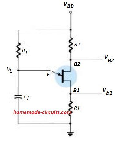
Here the components RT and CT work like the timing elements and determine the frequency or the oscillation rate of the UJT circuit.
For calculating the oscillating frequency we can use the following formula, which incorporates the unijunction transistor intrinsic stand-off ratio η as one of the parameters along with RT and CT for determining the oscillating pulses.

The standard value of the stand-off ratio for a typical UJT device is between 0.4 and 0.6. Thus considering the value of η = 0.5, and substituting it in the above equation we get:

When the supply is switched ON, the voltage through the resistor RT charges the capacitor CT towards the supply level VBB. Now, the stand-off voltage Vp is determined by Vp across B1 - B2, in conjunction with the UJT stand-off ratio η as: Vp = ηVB1VB2 - VD.
For so long the the voltage VE across the capacitor stays lower than the Vp, the UJT terminals across B1, B2 exhibits an open circuit.
But the moment the voltage across CT goes beyond Vp, the unijunction transistor fires, quickly discharging the capacitor, and initiating a fresh cycle.
During the firing instance of the UJT, results in the potential across R1 to rise, and the potential across R2 to drop.
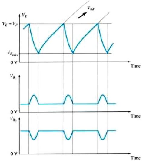
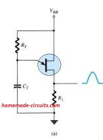
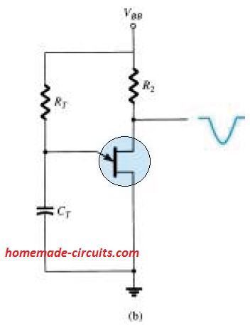
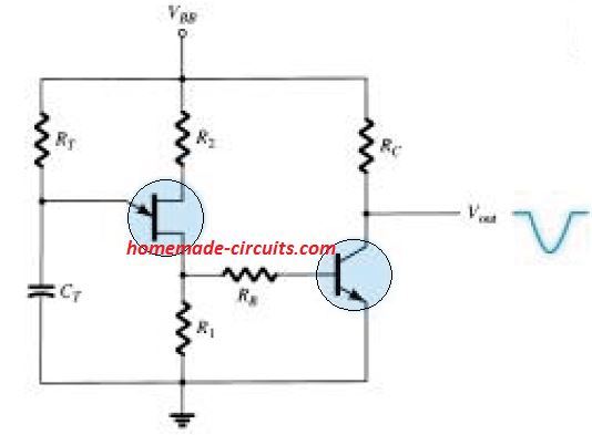
The resultant waveform across the emitter of the UJT produces a sawtooth signal, which exhibits a positive-going potential at B2, and a negative-going potential at B1 leads of the UJT
Application Areas of Unijunction Transistor
The following are the main application areas where unijunction transistors are widely used.
- Triggering Circuits
- Oscillators Circuits
- Voltage/Current Regulated supplies.
- Timer based Circuits,
- Sawtooth Generators,
- Phase Control Circuits
- Bistable networks
Main Features
Easily Accessible and Cheap: The cheap price and easy availability of UJTs along with some exceptional features has led to a wide implementation of this device in many electronic applications.
Low Power Consumption: Due to their a low power consumption feature under normal working conditions, the device is considered as an incredible breakthrough in the constant effort to develop reasonably efficient devices.
Highly Stable Reliable Operation: When used as an oscillator or in delay triggering circuit, the UJT works with extreme reliability and with an extremely accurate output response.
Unijunction Transistor Basic Construction
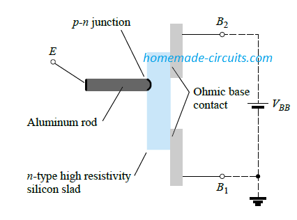
The UJT is a three-terminal semiconductor device which incorporates a simple construction as depicted in the above figure.
In this construction, a block of mildly doped n-type silicon material (having increased resistance characteristic) provides a pair of base contacts connected to two ends of one surface, and an aluminum rod alloyed on the opposite rear surface.
The p-n junction of the device is created on the border of the aluminum rod and the n-type silicon block.
This so formed single p-n junction is the reason for the name of the device "unijunction". The device was initially known as duo (double) base diode because of the occurrence of a pair of base contacts.
Notice that in the above figure that the aluminum rod is fused/merged on the silicon block at a position more close to the base 2 contact than the base 1 contact, and also the base 2 terminal has become positive with respect to the base 1 terminal by VBB volts. How these aspects influence the working of the UJT will be apparent in the following sections
Symbolic Representation
The symbolic representation of the unijunction transistor can be seen in the below image.
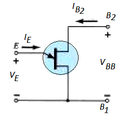
Observe that the emitter terminal is shown with an angle to the straight line which depicts the block of n-type material. The arrow head can be seen directing in the direction of typical current (hole) flow while the unijunction device is in the forward-biased, triggered, or conducting condition.
Unijunction Transistor Equivalent Circuit
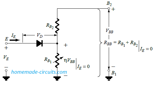
The equivalent UJT circuit can be witnessed in the above shown image. We can find how relatively simple this equivalent circuit appears to be, which includes a couple of resistors (one fixed, one adjustable) and a solitary diode.
The resistance RB1 is displayed as a adjustable resistor considering its value will change as the current IE changes. Actually, in any transistor that represents a unijunction, RB1 may fluctuate from 5 kΩ down to 50 Ω for any equivalent change of IE from 0 to 50 = μA. The interbase resistance RBB represents the resistance of the device between terminals B1 and B2 when IE = 0. In formula for this is,
RBB = (RB1 + RB2)| IE = 0
The range of RBB is normally within 4 and 10 k. The aluminum rod placement as shown in the first figure provides the relative magnitudes of RB1, RB2 when IE = 0. We can estimate the value of VRB1 (when IE = 0) using the voltage-divider law, as given below:
VRB1 = (RB1 x VBB) / (RB1 + RB2) = ηVBB (with IE = 0)
The Greek letter η (eta) is known as the intrinsic stand-off ratio of the unijunction transistor device and is defined by:
η = RB1 / (RB1 + RB2)( with IE = 0) = RB1 / RBB
For the indicated emitter voltage (VE) higher than VRB1( = ηVBB) by the diode's forward voltage drop VD (0.35 → 0.70 V), the diode will get triggered ON. Ideally we may assume the short-circuit condition, such that IE will start to conduct via RB1. Through equation, the triggering voltage level of the emitter can be expressed as:
VP = ηVBB + VD
Main Characteristics and Working
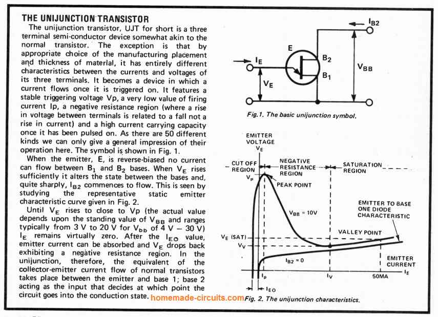
The characteristics of a representative unijunction transistor for VBB = 10 V is indicated in the figure below.
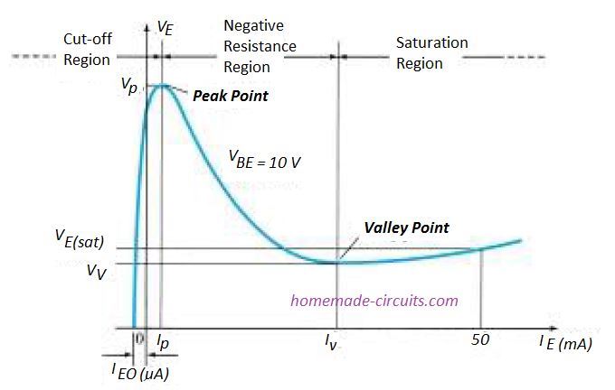
We can see that, for emitter potential indicated at the left side of the peak point, the IE value never exceeds the IEO (which is in microamperes). The current IEO more or less follows the reverse leakage current ICO of the conventional bipolar transistor.
This region, is referred to as the cutoff region, as also indicated in the fig.
As soon as conduction is achieved at VE = VP, the emitter potential VE decreases as IE potential increases, which is precisely in accordance with the decreasing resistance RB1 for increasing current IE, as explained previously.
The above characteristic provides a unijunction transistor with a highly stable negative resistance region, that enables the device to work and to be applied with extreme reliability.
During the above process, the valley point could be expected to be finally attained, and any increase in IE beyond this range causes the device to enter the saturation region.
The figure #3 shows a diode equivalent circuit in the same region with a similar characteristics approach.
The drop in the resistance value of the device in the active region is caused on account of the injected holes into the n-type block by the p-type aluminum rod as soon as the firing of the device happens. This results in an increase in the quantity of holes on the n-type section increases the free electrons number, causing an enhanced conductivity (G) across the device with an equivalent decrease in its resistance (R ↓ = 1/G ↑)
Important Parameters
You will find three additional important parameters associated with a unijunction transistor which are IP, VV, and IV. All of these are indicated in the figure #4.
These are actually quite easy to understand. The normally existing emitter characteristic can be learned from below figure #5.
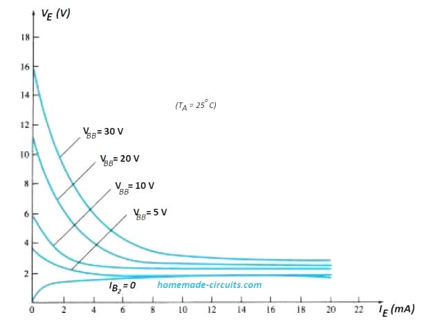
Here we can observe that IEO(μA) is unnoticeable because the horizontal scale is calibrated in milliamperes. Each of the curve intersecting the vertical axis is the corresponding results of VP. For constant values of η and VD, the VP value changes in accordance with VBB, as formulated below:

Unijunction Transistor Datasheet
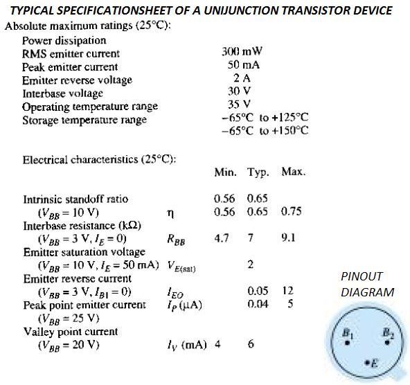
A standard range of technical specs for the UJT can be learned from Figure #5 below.
UJT Pinout Details
The pinout details is also included in the above datasheet. Notice that the base terminals B1 and B2 are situated opposite to each other while the emitter pin E is positioned at the center, between these two.
Moreover, the base pin which is supposed to be connected with higher supply levels is situated near to the off shoot on the collar of the package.
How to use an UJT for Triggering an SCR
One relatively popular application of the UJT is for triggering power device such as the SCR. The fundamental components of this type of triggering circuit is depicted in the below shown diagram #6.
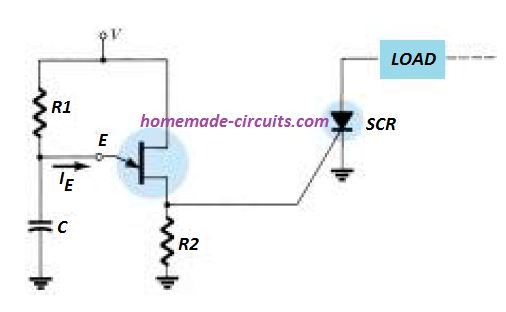
The main timing components are formed by R1 and C, while R2 works like a pull down resistors for the output triggering voltage.
How to Calculate R1
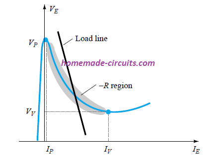
The resistor R1 has to be calculated to guarantee that the load line as defined by R1 travels via the device's characteristics within the negative resistance region, meaning, towards the right side of the peak point but to the left side of the valley point as indicated in Fig #7.
If the load line isn't able to cross the right side of the peak point, the unijunction device cannot start up.
The R1 formula which guarantees a switch ON condition could be determined once we take into account the peak point where IR1 = IP and VE = VP. The equation IR1 = IP looks logical because the capacitor's charging current, at this point, is zero. Meaning , the capacitor at this specific point is transiting through a charging to a discharging condition.
For the above condition we can therefore write:
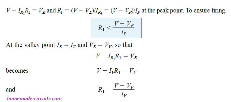
Alternatively, in order to guarantee a complete SCR turn off :
R1 > (V - Vv) / Iv
This implies that the selection range of the resistor R1 has to be as expressed as given below:
(V - Vv) / Iv < R1 < (V - Vp) / Ip
How to Calculate R2
The resistor R2 must be adequately small to ensure that the SCR is not falsely triggered by voltage VR2 across R2 when IE ≅ 0 Amp. For this the VR2 must be calculated as per the following formula:
VR2 ≅ R2V / (R2 + RBB) (when IE ≅ 0)
The capacitor provides the time delay between the triggering pulses, and also determines the length of each pulse.
How to Calculate C
Referring to the figure below, as soon as the circuit is powered, the voltage VE which is equal to VC will begin charging the capacitor towards voltage VV, through a time constant τ = R1C.
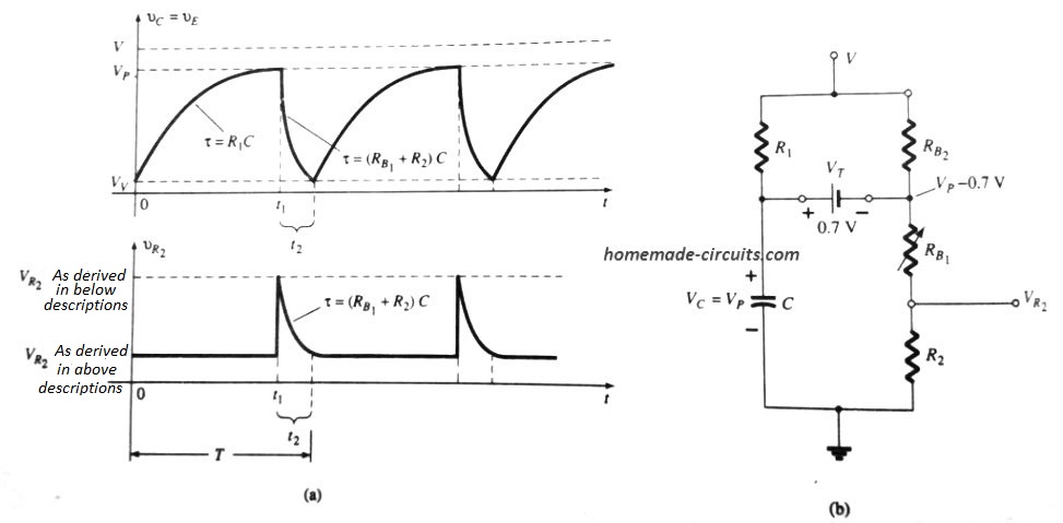
The general equation that determines the charging period of C in a UJT network is:
vc = Vv + (V - Vv)( 1 - e-t/R1C)
Through our previous calculations we already know the volatge across R2 during the above charging period of the capacitor. Now, when vc = vE = Vp, the UJT device will get into switch ON state, causing the capacitor to discharge via RB1 and R2, with a rate depending on the time constant:
τ = (RB1 + R2)C
The following equation can be used for calculating discharge time when
vc = vE
vc ≅ Vpe-t/(RB1 + R2)C
This equation has turned a bit complex due to RB1, which goes through a decrease in value as the the emitter current increases, along with other aspects in the circuit like R1 and V, which also affect the discharge rate of C overall.
Despite of this, if we refer to the equivalent circuit as given above Figure #8 (b), typically the values of R1 and RB2 can be such that a Thévenin network for the configuration around the capacitor C might be marginally affected by the R1, RB2 resistors. Although the voltage V appears to be rather large, the resistive divider aiding the Thévenin voltage could be generally overlooked and eliminated, as shown in the below reduced equivalent diagram:
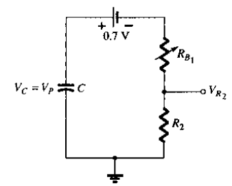
Therefore, the simplified version above helps us to get the following equation for the discharge phase of the capacitor C, when VR2 is at its peak.
VR2 ≅ R2(Vp - 0.7) / R2 + RB1
For more application circuits you may also refer to this article
Good explanation but the procedure to obtain the period of the pulse was not clear . Please put more equation on how to establish the period of the pulse and hence the frequency