In this post I have explained s few simple DC to DC buck-boost converter circuits which can be used for either stepping up the input DC voltage or stepping down the input DC voltage to specific output DC voltage levels.
Since a buck-boost converter allows the input voltage to be either stepped up or stepped down, hence it is named as buck and boost converter or buck-boost converter.
Basic Working principle
The basic working principle of a buck-boost converter can be understood with the help of the following explanation.
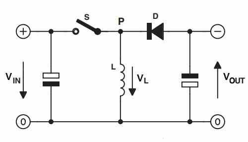
Referring to the basic buck-boost topology diagram above, when the switch S is closed, the input voltage VIN is blocked by the diode D, since D is reverse biased. Therefore the voltage has no other option but to flow through the inductor L.
The inductor L due to its inherent reluctance property initially tries to block the current. Due to this, initially the voltage drop across L is high. However, slowly as the reluctance of the coil decreases and the current through the inductor increases.
During this phase the inductor L stores the energy (voltage and current) inside its winding.
Ideally this the point when the switch S needs to be opened.
When switch S is now opened, the voltage VL stored inside the inductor reverses direction, and it passes through the diode D which is now forward biased. In the process VL also passes through the output capacitor and charges it fully.
During this phase the output capacitor stores energy inside it and gets fully charged, simultaneously the load across VOUT also gets the energy from the inductor for ts operation.
Next, at this point if the switch is closed again, the process repeats as explained above, however now the capacitor provides its stored energy to the load.
Depending how how fast or how slow the switch S is closed and opened, the output DC can be a stepped up or boosted output, or it can be a stepped down or buck output.
In a real life electronic buck-boost circuit, the switch S is replaced with a BJT or a MOSFET and this device is switched ON/OFF through an external PWM for generating a buck or a boost output.
Simple Two Transistor Buck-Boost Converter Circuit
The following figure shows how a very simple buck-boost converter could be built using just a couple of transistors and a few other passive parts.
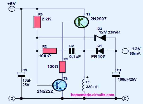
The working of the circuit can be understood from the following points:
Here the circuit is configured to provide a negative boosted output from a 5V input to a -12V output.
As soon as the circuit is powered, the T2 switches ON via R3. This allows T1 to also switch ON through the negative base bias received via R1 and T2.
This causes the full +5V to be applied across the inductor L1 via the collector of T1.
The inductor, due to it reluctance opposes the instant rise in current across it and in the process begins storing energy inside its winding.
Now, slowly the inductor reluctance drops and it starts passing more and more current through. Due to this the base current of T2 is pulled to ground through the inductor and via R2 and C2.
This causes T2 to shut off momentarily.
Now, the stored energy inside the inductor is released back to the output across C1.
C1 now charges fully and simultaneously the output is also supplied with a negatively boosted voltage.
The 12 V diode makes sure that the inverted output boosted voltage does not rise above -12V.
Subsequently C2 begins charging until it is fully charged, which allows T2 to switch ON again, and the process repeats. This repetition process continues at a high frequency.
The frequency of the converter is determined basically by the values of R2 and C2.
By appropriately tweaking the values of R2 and C2, this two transistor circuit could be optimized either to work like a buck converter or a boost converter.
Using IC 555 for the Buck-Boost
This highly efficient and effective buck-boost circuit using the work horse IC 555 would allow you to convert an input source voltage to any required degree, either bucked or boosted, as desired.
We have already learned the concept comprehensively through one of my previous articles where I have explained the versatility of this buck-boost type of topology.
As shown in the circuit diagram below (click to enlarge) the configuration is basically a combination of two distinct stages, viz the upper buck-boost converter stage and the lower IC 555 PWM controller stage.
The buck-boost stage consists of a mosfet which acts like a switch, the inductor which is the main power converting component, the diode which just like the mosfet forms a complementary switch, and the capacitor quite like the inductor forms a complementary power converter device.
The mosfet needs to operate through pulsed triggering so that it alternately switches the input voltage ON and OFF across the inductor in response to its gate voltage.
Therefore the gate voltage should also be in a pulsed form which is accomplished through a IC555 PWM generator stage.
Circuit Operation
The associated IC555 PWM generator is integrated to the mosfet for accomplishing the above discussed operation.
During the ON time of the mosfet, the input voltage is allowed to pass through the mosfet and is applied right across the inductor.
The inductor owing to its inherent property tries to counter this sudden infliction of current by absorbing and storing the power in it.
During the subsequent OFF period of the mosfet, the input voltage is shut off by the mosfet, the inductor now experiences a sudden change in current from peak to zero. In response, the inductor counters this by reversing its stored power across the output terminals via the diode which now acts in the forward biased condition.
The above power from the inductor appears with opposite polarity across the output where the intended load is connected.
The capacitor is positioned to store a portion of the power in it, so that it can be used by the load during the ON time of the mosfet when the diode is reverse biased and power cut off across the load.
This heps to maintain a steady and stable voltage across the load during both ON and OFF cycles of the mosfet.
Using PWM as the Controller
The level of voltage, whether it's a boosted voltage or bucked voltage depends upon how the mosfet is controlled by the PWM generator.
If the mosfet is optimized with higher ON time than the OFF time then the output would generate boosted voltage and vice versa.
However there may be a limit to this, care must be taken not to exceed the ON time beyond the full saturation time of the inductor, and the OFF time must not be below the minimum saturation time of the inductor.
For instance suppose it takes 3ms for the inductor to become fully saturated, the ON time in this case can be set within 0 - 3ms, and not beyond that, This will result in a boost from minimum to maximum depending upon the value of the chosen inductor.
The associated pot wit the IC555 PWM generator can be effectively tweaked for acquiring any desired buck-boost voltage at the output.
The inductor value is a matter of trial and error, try to incorporate as many winding as possible for acquiring better and efficient results and diverse range.
Circuit Diagram
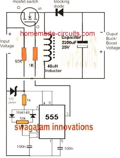
The above design can be suitably upgraded for implementing an automatic output voltage correction with the help of the following modifications:
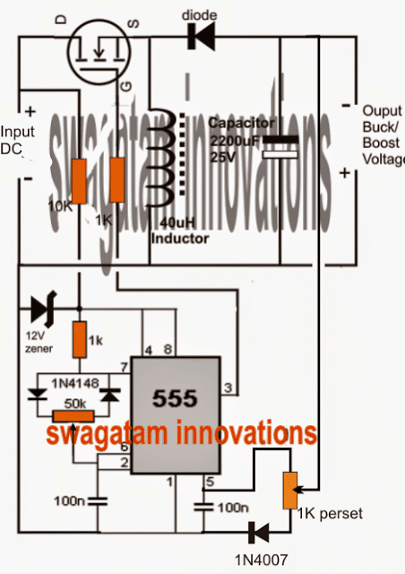
The 1K preset may be appropriately set initially for determining the desired control point.
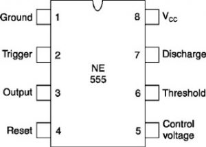
IC 555 Pinouts
