In this post I have explained an enhanced multi-spark CDI circuit which is universally suited for all types of automobiles. The unit can be built at home and installed in a particular vehicle for achieving greater speed to fuel efficiency.
The Circuit Concept
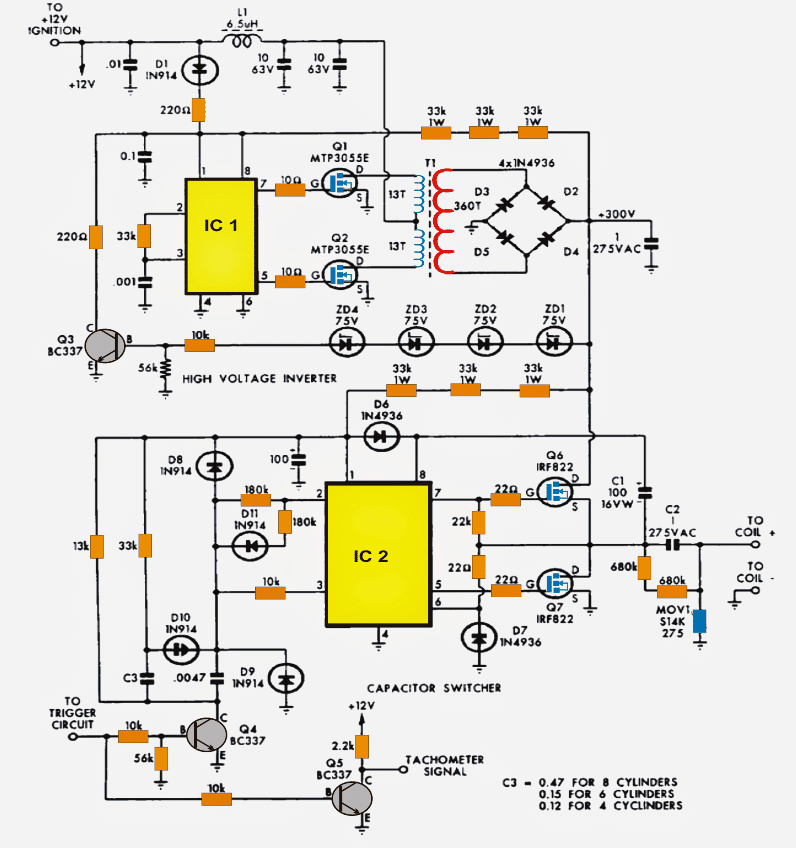
The following diagram illustrates an enhanced version of a multi-spark CDI circuit. Fundamentally it can bifurcated into two discrete stages.
Both the stages incorporate the IC IR2155 MOSFET driver with built in 50% duty cycle oscillator.
The upper stage consisting of Q1, Q2 are configured for generating 300V DC from the available 12V DC input battery supply.
The IC2 along with the connected mosfets Q6/Q7 form a push pull type pump circuit for alternately charging and discharging a high voltage capacitor across the connected ignition coil.
Circuit Operation
IC1 is wired up for oscillating at about 22kHz as per the selection of the 33k resistor and the 102 capacitor across pin2/3 and pin3/ground respectively.
This results in producing alternate switching of its output mosfetsQ1/Q2 connected across pins 5/7.
The above switching performs a push pull reaction over the connected transformer wherein the two halves of the winding are saturated alternately with the mosfet conduction, which results in pumping of the entire 12V DC across the two half winding of the transformer.
This action results in a stepped up induction across the secondary winding of the transformer giving rise to the required 300V AC switched at the 22kHz rate.
The mosfets have their own internal transient protection system built in in the form of 60V zener diodes which limit the internal spikes to 60V safeguarding them from the relevant dangers, also the external gate 10 ohm resistors ensures a relatively exponential charge and discharge of the mosfet internal capacitance thereby reducing noise and disturbance which could otherwise influence the vehicle electrical adversely.
A couple metalized capacitors rated at 10uF are installed in order to decouple DC from T1 so that Tr1 receives the 12V switching optimally across its winding.
The stepped up voltage at the output of TR1 is rectified by the 4 fast recovery type diodes configured as a bridge rectifier.
The ripples are further filtered by the metalized high voltage capacitor rated at 1uF/275V
Even with the all the above high efficiency and protected circuitry, the IC1 stage has no ability os controlling the output voltage in response to the rising and falling of the 12V DC input which normally wouldn't be stable due to the vehicle's speeds and alternator RPM variations.
To tackle this, an innovative transformer output voltage correction feature is Incorporated here using a voltage feedback circuitry involving ZD1---ZD4 along with Q3 and a few passive components.
The four 75V zeners start conducting as soon as the voltage begins drifting above the 300V mark, which in turn results in the conduction of Q3. This action from Q3 results in dragging pin1 voltage of IC1 from 12V to gradually 6V.
Using the Shut Down Option
Pin1 being the shut down pinout of the IC1 alerts the IC to trigger its internal under voltage cut-off feature resulting in an instantaneous shut down of its output pulses which in turn switches off the mosfets for that particular instant.
The mosfets being switched OFF means no output voltage and Q3 unable to conduct which again restores the circuit to its original functional mode, and the operations repeat and rotate keeping the output voltage quite stabilized at the specified 300V volt mark.
Another clever enhancement technique employed here is the use of three 33k resistors feedback loop from the output of TR1 to the IC1 supply pinout.
This loop ensures that the circuit stays functional even when the vehicle is not running at optimal speeds or the supply voltage dropping considerably below the required 12V level.
During such situations, the discussed 33kx3 feedback loop keeps the voltage level to IC1 well above 12V ensuring optimal response even under conditions with steep voltage falls.
The 300V from TR1 is also applied to IC2 which is specifically configured as a high side mosfet driver, because here its output is not connected with a center tap transformer rather a single coil which needs a full drive across its winding in forward reverse method during each alternate pulse from IC2.
Thanks to the IC IR2155 which has all the necessary features built in and effectively starts working as a high side driver with the help of just a few external passive parts C1, C6, D7.
Function of the Ferrite Transformer
The conduction of Q6/Q7 pumps the 300V volts from TR1 inside the connected ignition coil primary via the 1uF/275V capacitor.
The calculated configuration of various components across pin2 and pin3 of IC2 constitutes the intended multi sparks across the connected coil due to the interactions between these components. More precisely, the parts form a timer design with the help of the 180k resistor at pin2 along with the 0.0047uF capacitor across pin3 of IC2.
The 10k resistor and the 0.0047uF capacitor between pin3 restricts over current while it's being triggered by the MMV circuit.
The output from Q5 facilitates a low voltage output for integrating a tachometer in order to provide valid readings on the meter rather than connecting directly to the spark plug.
If in case the multi spark feature seems not so useful or for some reasons inappropriate then it can be successfully disabled by eliminating C3, D10, D11 and the couple of 180k resistors along with the 33k and the 13k resistors. Also by substituting the 33k resistor with a 180 k resistor and a short link in place of D10.
The above mods will force IC2 to generate just single 0.5ms pulses as soon as Q7 is triggered. The ignition coil now fires only in one direction while Q7 is ON and in once in the opposite direction when Q6 is ON.
The associated MOV neutralizes any possibility of high voltage transients in case the output of the ignition coil is left open.
The couple of 680k resistors across C2 provides a safe discharging path for C2 whenever the coil is disconnected from the circuit.
This safeguards the circuit and the user from nasty high voltage discharge from C2.
Circuit Diagram

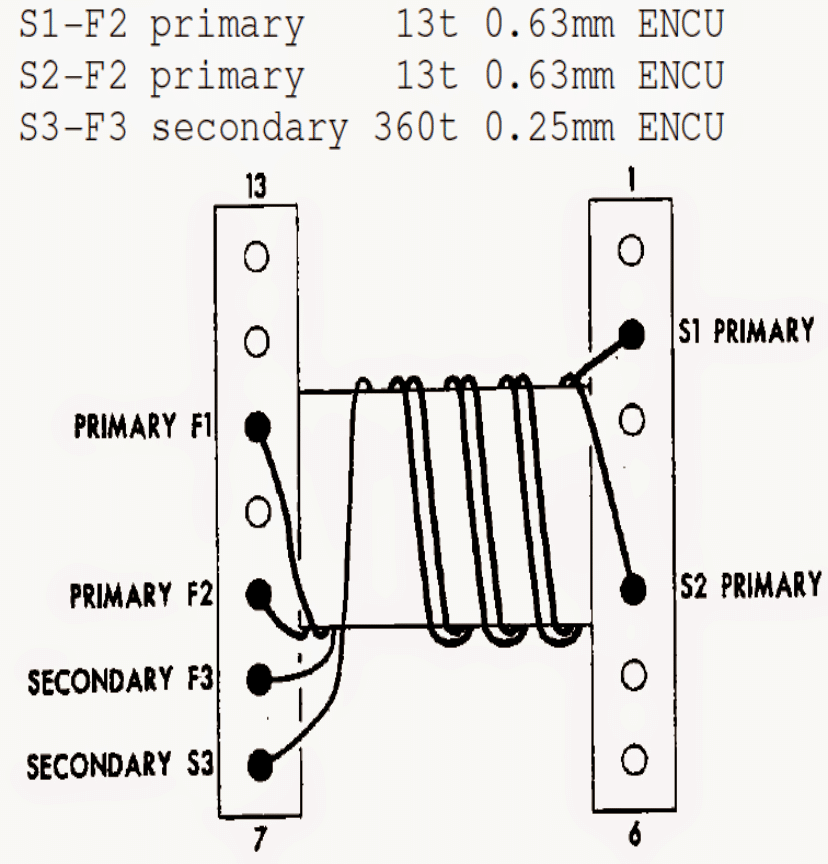
TR1 winding Details:
Start from pin7 (left hand side) using 0.25mm enameled super enameled copper wire as shown in the diagram and end at pin8(left hand side) with 360 turns.
This completes the secondary winding.
For the primary side wind in a bifilar manner meaning wind both the winding together, starting at pin2 and pin4 (right hand side) and ending after 13 turns at pin11 and pin9 respectively (left hand side) using 0.63mm wire.
The bobbin used is for suiting N27 Ferrite Core
L1 is 12 turns of 1mm wire on a Neosid Ringcore 17-732-22
Transformer Design
