

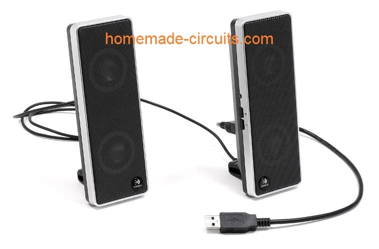
Audio amplifiers which are designed to work with a 5 V supply from a USB socket such as from a computer USB are called an USB amplifiers.
In this article I have explained how to build a simple 3 watt amplifier circuit which can be powered directly from a computer 5V USB port for driving an 8 ohm 3 watt speaker. You can build a couple of such circuits and use them for creating a stereo output into a pair of 8 Ohm speakers.
Please note that TDA2822 IC is obsolete now therefore opting a circuit using this IC for the discussed project may not be a good idea. However the present design is based on the IC LM4871, which is abundantly available I have explained the main features and working of this IC

Main Features
- The IC works without involving any sort of coupling capacitors, or bootstrap capacitors, or snubber capacitors
- It exhibits extreme stability through Unity Gain .
- Comes with WSON, VSSOP, SOIC, or PDIP Packaging
- Allows to Set an external Gain control network
Important Specifications:
- The IC LM4871D is designed to handle loudspeakers rated at 3 ohms or 4 ohms at 3 watts
- All the remaining versions in the series are specified to handle 1.5 watt with 8 Ohm speaker.
- The ICs have shutdown current internally set at 0.6uA typically
- The working voltage range is between 2.0V to 5.5V, perfectly suited to work with PC USB power.
- Maximum Total Harmonic Distortion with a 8 Ohm speaker load at 1kHz is around 0.5%
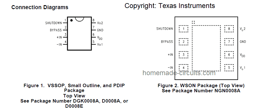
Pinout Specifications and Package
The following image shows the pinout details of the IC and the available package models, and layouts:

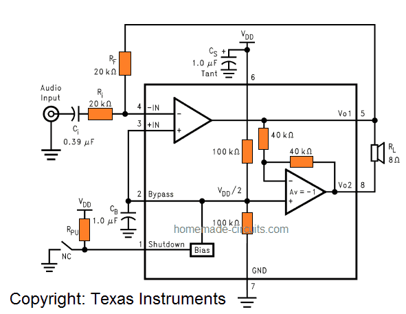
5V USB Amplifier Circuit Operation

Parts List
All resistors 1/4 watt or 1/8 watt, 1% MFR or SMD
- 20 K = 2 nos
- 100 K = 1 no (Rpu)
Capacitors
- 0.39uF ceramic = 1 no
- 1uF / 16V Tantalum = 2 nos
Semiconductor
IC LM4871 = 1 no
As can be seen in the above schematic, the LM4871 includes a couple of operational amplifiers internally, providing the user the option of configuring the amplifier through a few specified ways.
The gain of the first amplifier can be managed externally, while the second amplifier has been wired up internally with an inverting unity gain.
The closed loop gain for the first amplifier can be determined by appropriately selecting the values of the ratio Rf/Ri, whereas the same has been fixed for the second amplifier internally through a couple of 40K resistors.
We can see that the output of the amplifier#1 is configured to be the input of amplifier#2, allowing both the amplifiers to generate signals with identical values, although these may be 180 degrees out of phase.
This results in the IC’s differential gain to be AVD= 2 *(Rf /Ri ) .
Typically, for any amplifier a “bridged mode” set up can be implemented by driving the connected load deferentially via a couple of outputs Vo1 and Vo2.
An amplifier configured in the bridged mode will have a different operating principle in contrast to the traditional single ended amplifiers which have one end of the load wired with the ground line.
A bridged mode circuit works with better efficiency compared to a single ended amplifier since the load or the loudspeaker is switched in a push-pull manner, enabling a double voltage swing for each alternate frequency pulse.
This actually allows the loudspeaker to produce 4 times more power than a single ended version under identical circumstances or specifications.
The ability to achieve such increased power allows the amplifier to work without a current limiter stage and hence without undesirable clipping.
An added benefit of differential bridged output is the absence of net DC across the connected loudspeaker. This happens since VO1 and VO1 are biased at identical voltage levels, that is VDD/2 in the present case. This allows the amplifier to work without an output coupling capacitor, which otherwise becomes mandatory in single ended amplifiers.
Understanding Component Working and Specifications
Ri is the inverting input resistor which is employed to set the closed loop gain along with Rf. Additionally this resistor also implements a high pass filter function with Ci at fC= 1/(2π RiCi).
Ci forms the input coupling capacitor positioned to block DC and allow audio AC frequency across the input pins. This capacitor also enables a high pass filter in conjunction with Ri at fC= 1/(2π RiCi).
Rf becomes the feedback resistance that fixes the closed loop gain with the help of Ri.
Cs acts like supply bypass capacitor and provides ripple filtering for the power supply.
Cb is positioned as the bypass pin capacitor and this capacitor enforces filtering for half-supply
Absolute Maximum Ratings
The maximum tolerable rating for this circuit are I have explained below:
- Maximum supply voltage is 6V, typical working voltage is 5V
- The minimum and maximum tolerable temperature levels are -65 and 150 degrees Celsius respectively.
- The input music signal from the USB could be anywhere between -0.3V and 5.3 V
- Maximum power dissipation is internally limited so no need to worry about this issue.
Electrical Characteristics:
Vdd signifies the supply voltage which is within 2V and 5.5V typically.
Idd is the quiescent current consumed from the input power supply by the IC and this may lie between 6.5mA to 10mA
Isd is the symbol for shutdown current, when pin#1 potential becomes equal to Vdd, the shutdown is initiated causing the consumption to drop to 0.6uA
Vos refers to output offset voltage, and is initiated when Vin = 0V, and could be 5V typically, and 50mV in the limited mode.
P0 is the output power and is around 3 watts when the load is an 3 or 4 Ohm speaker
THD+N indicates the total harmonic distortion which is within 0.13 to 0.25% with a frequency range of 20Hz to 20kHz.
PSRR gives us the power supply rejection ratio for Vdd at 5V typical, and this is around 60dB.
Prototype Image of the 5V USB amplifier:

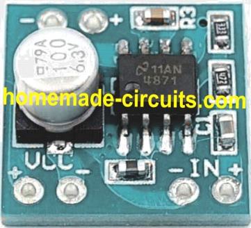
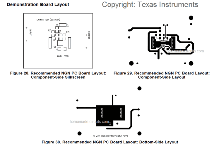
PCB Layout Recommendation:

Original article: www.ti.com/lit/ds/symlink/lm4871.pdf